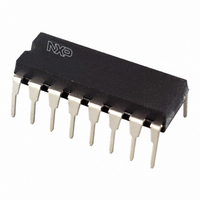
TEA1062A/C4/M1,112 NXP Semiconductors, TEA1062A/C4/M1,112 Datasheet - Page 5

TEA1062A/C4/M1,112
Manufacturer Part Number
TEA1062A/C4/M1,112
Description
IC TRANSMISSION LV 16-DIP
Manufacturer
NXP Semiconductors
Datasheet
1.TEA1062AC4M1112.pdf
(28 pages)
Specifications of TEA1062A/C4/M1,112
Function
Low Voltage Transmission
Number Of Circuits
1
Voltage - Supply
3.4V
Current - Supply
900µA
Power (watts)
666mW
Operating Temperature
-25°C ~ 75°C
Mounting Type
Through Hole
Package / Case
*
Includes
MUTE, Receiving Amplifier, Voltage Regulation
Lead Free Status / RoHS Status
Lead free / RoHS Compliant
Interface
-
Other names
935230190112
TEA1062AM1N
TEA1062AM1N
TEA1062AM1N
TEA1062AM1N
Philips Semiconductors
FUNCTIONAL DESCRIPTION
Supplies V
Power for the IC and its peripheral circuits is usually
obtained from the telephone line. The supply voltage is
derived from the line via a dropping resistor and regulated
by the IC. The supply voltage V
supply external circuits e.g. dialling and control circuits.
Decoupling of the supply voltage is performed by a
capacitor between V
regulator is decoupled by a capacitor between REG and
V
The DC current flowing into the set is determined by the
exchange supply voltage V
resistance R
line R
The circuit has an internal current stabilizer operating at a
level determined by a 3.6 k resistor connected between
STAB and V
more than 0.5 mA greater than the sum of the IC supply
current (I
circuitry connected to V
shunted to V
The regulated voltage on the line terminal (V
calculated as:
V
reference voltage of 3.7 V and R9 is an external resistor
connected between SLPE and V
In normal use the value of R9 would be 20 .
Changing the value of R9 will also affect microphone gain,
DTMF gain, gain control characteristics, sidetone level,
maximum output swing on LN and the DC characteristics
(especially at the lower voltages).
Under normal conditions, when I
the static behaviour of the circuit is that of a 3.7 V regulator
diode with an internal resistance equal to that of R9. In the
audio frequency range the dynamic impedance is largely
determined by R1. Fig.3 shows the equivalent impedance
of the circuit.
1997 Sep 03
EE
ref
V
V
Low voltage transmission circuits with
dialler interface
.
LN
LN
is an internally generated temperature compensated
line
= V
= V
.
CC
ref
ref
) and the current drawn by the peripheral
CC
EE
exch
EE
+ I
+ {(I
, LN, SLPE, REG and STAB
SLPE
(see Fig.9). When the line current (I
via LN.
and the DC resistance of the telephone
line
CC
I
R9
CC
CC
and V
(I
exch
0.5
p
) the excess current is
EE
, the feeding bridge
CC
. The internal voltage
SLPE
EE
10
may also be used to
.
3
>> I
A)
CC
I
p
+ 0.5 mA + I
}
LN
) can be
R9
line
) is
p
,
5
At line currents below 9 mA the internal reference voltage
is automatically adjusted to a lower value (typically 1.6 V
at 1 mA). This means that more sets can be operated in
parallel with DC line voltages (excluding the polarity guard)
down to an absolute minimum voltage of 1.6 V. At line
currents below 9 mA the circuit has limited sending and
receiving levels. The internal reference voltage can be
adjusted by means of an external resistor (R
This resistor when connected between LN and REG will
decrease the internal reference voltage and when
connected between REG and SLPE will increase the
internal reference voltage.
Current (I
depends on the external components used. Fig.10 shows
this current for V
MUTE is HIGH (TEA1062A) when the receiving amplifier
is driven, the available current is further reduced. Current
availability can be increased by connecting the supply IC
(TEA1081) in parallel with R1 as shown in Fig.19 and
Fig.20, or by increasing the DC line voltage by means of
an external resistor (R
SLPE (Fig.18).
handbook, halfpage
L
R
eq
p
= 16.2 k .
= C3
p
V
) available from V
Fig.3 Equivalent impedance circuit.
LN
EE
R9
R
CC
p
.
2.2 V. If MUTE is LOW (TEA1062) or
R9
20
L eq
VA
TEA1062; TEA1062A
V ref
) connected between REG and
CC
for peripheral circuits
R p
REG
C3
4.7 F
Product specification
MBA454
R1
V CC
C1
100 F
VA
).


