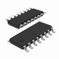
SI3019-KS Silicon Laboratories Inc, SI3019-KS Datasheet - Page 10

SI3019-KS
Manufacturer Part Number
SI3019-KS
Description
IC VOICE DAA GCI/PCM/SPI 16SOIC
Manufacturer
Silicon Laboratories Inc
Type
Chipsetr
Datasheet
1.SI3056-KS.pdf
(96 pages)
Specifications of SI3019-KS
Package / Case
16-SOIC (3.9mm Width)
Function
Data Access Arrangement (DAA)
Interface
GCI, PCM, SPI
Number Of Circuits
1
Voltage - Supply
3 V ~ 3.6 V
Current - Supply
8.5mA
Operating Temperature
0°C ~ 70°C
Mounting Type
Surface Mount
Includes
Line Voltage Monitor, Loop Current Monitor, Overload Detection, Parallel Handset Detection, Polarity Reversal Detection, TIP and
Product
Modem Chip
Supply Voltage (min)
3 V
Supply Current
8.5 mA
Maximum Operating Temperature
+ 70 C
Minimum Operating Temperature
0 C
Mounting Style
SMD/SMT
Lead Free Status / RoHS Status
Contains lead / RoHS non-compliant
Power (watts)
-
Lead Free Status / RoHS Status
Lead free / RoHS Compliant, Contains lead / RoHS non-compliant
Available stocks
Company
Part Number
Manufacturer
Quantity
Price
Part Number:
SI3019-KS
Manufacturer:
SILICON LABS/芯科
Quantity:
20 000
Company:
Part Number:
SI3019-KSR
Manufacturer:
SILICONLAB
Quantity:
2 722
Si3018/19/10
Table 5. Absolute Maximum Ratings
10
Table 6. Switching Characteristics—General Inputs
(V
Parameter
DC Supply Voltage
Input Current, Si3056 Digital Input Pins
Digital Input Voltage
Operating Temperature Range
Storage Temperature Range
Note: Permanent device damage can occur if the above absolute maximum ratings are exceeded. Restrict functional
Parameter
Cycle Time, MCLK
MCLK Duty Cycle
MCLK Jitter Tolerance
Rise Time, MCLK
Fall Time, MCLK
MCLK Before RESET ↑
RESET Pulse Width
M0, M Before RESET↑
Notes:
D
RESET
M 0, M1
=
1. All timing (except Rise and Fall time) is referenced to the 50% level of the waveform. Input test levels are
2. The minimum RESET pulse width is the greater of 250 ns or 10 MCLK cycle times.
3. M0 and M are typically connected to V
M CLK
3.0 to 3.6 V, T
operation to the conditions as specified in the operational sections of this data sheet. Exposure to absolute maximum
rating conditions for extended periods might affect device reliability.
V
IH
=
1
V
D
– 0.4 V, V
A
=
2
70 °C for K-Grade, C
3
IL
=
0.4 V. Rise and fall times are referenced to the 20% and 80% levels of the waveform.
Figure 2. General Inputs Timing Diagram
L
D
=
or GND and should not be changed during normal operation.
20 pF)
Symbol
T
V
Rev. 1.03
Symbol
V
I
T
STG
IND
IN
D
A
t
t
t
t
t
rl
jitter
t
mxr
mc
dty
t
mr
t
t
rl
r
f
t
t
m xr
r
16.67
Min
250
40
10
20
—
—
—
t
–0.3 to (V
m r
–0.5 to 3.6
–40 to 100
–65 to 150
t
m c
Value
±10
D
Typ
50
+ 0.3)
—
—
—
—
—
—
—
1000
Max
60
±2
—
—
—
5
5
t
f
Unit
mA
°C
°C
V
V
cycles
Unit
ns
ns
ns
ns
ns
ns
%
V
V
IH
IL


