SCC2691AC1A28,602 NXP Semiconductors, SCC2691AC1A28,602 Datasheet - Page 11
SCC2691AC1A28,602
Manufacturer Part Number
SCC2691AC1A28,602
Description
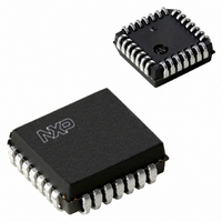
IC UART SINGLE 28-PLCC
Manufacturer
NXP Semiconductors
Datasheet
1.SCC2691AC1A28623.pdf
(25 pages)
Specifications of SCC2691AC1A28,602
Features
False-start Bit Detection
Number Of Channels
1, UART
Fifo's
3Bit
Voltage - Supply
5V
With Auto Flow Control
Yes
With False Start Bit Detection
Yes
With Cmos
Yes
Mounting Type
Surface Mount
Package / Case
28-PLCC
Lead Free Status / RoHS Status
Lead free / RoHS Compliant
Other names
568-1212-5
933811550602
SCC2691AC1A28
933811550602
SCC2691AC1A28
Available stocks
Company
Part Number
Manufacturer
Quantity
Price
Company:

Part Number:
SCC2691AC1A28,602
Manufacturer:
NXP Semiconductors
Quantity:
10 000


Philips Semiconductors
Table 2.
2006 Aug 04
MR1 (Mode Register 1)
NOTE:
*In block error mode, block error conditions must be cleared by using the error reset command (command 4x) or a receiver reset.
MR2 (Mode Register 2)
NOTE: *Add 0.5 to values shown for 0–7 if channel is programmed for 5 bits/character.
CSR (Clock Select Register)
See Table 6 for BRG Test frequencies in this data sheet, and “Extended baud rates for SCN2681, SCN68681, SCC2691, SCC2692, SCC68681
and SCC2698B” Philips Semiconductors ICs for Data Communications, IC-19, 1994.
CR (Command Register)
NOTE:
Access to the miscellaneous commands should be separated by 3 X1 clock edges. A disabled transmitter cannot be loaded.
SR (Channel Status Register)
NOTE:
*These status bits are appended to the corresponding data character in the receive FIFO. A read of the status register provides these bits [7:5]
command (command 4x) or a receiver reset.
ACR (Auxiliary Control Register)
ISR (Interrupt Status Register)
IMR (Interrupt Mask Resister)
Received Break
from the top of the FIFO together with bits [4;0]. These bits are cleared by a reset error status command. In character mode they are reset when
RxRTS Control
the corresponding data character is read from the FIFO. In block error mode, block error conditions must be cleared by using the error reset
Universal asynchronous receiver/transmitter (UART)
MPI Change
Interrupt
BRG Set
0 = Set 1
1 = Set 2
MPI Pin
Change
1 = Yes
1 = Yes
Bit 7
1 = yes
0 = No
0 = No
0 = Off
1 = On
0 = no
Select
11 = Remote loop
01 = Auto echo
10 = Local loop
00 = Normal
*
Channel Mode
Register Bit Formats
Current State
RxINT Select
Miscellaneous Commands
0 = RxRDY
1 = FFULL
MPI Level
Interrupt
Framing
1 = High
MPI Pin
0 = Low
1 = Yes
Receiver Clock Select
0 = Off
1 = On
0 = No
Bit 6
Error
*
See Text
See Text
Mode and Source
Counter/Timer
Error Mode*
Not used
Not used
1 = Block
Control
0 = Char
See Text
TxRTS
1 = Yes
1 = Yes
0 = No
0 = No
Parity
Bit 5
Error
*
CTS Enable
Ready Int
Overrun
Counter
Counter
1 = Yes
1 = Yes
1 = Yes
0 = No
Ready
0 = Off
1 = On
0 = No
0 = No
Bit 4
Error
11 = Special mode
00 = With parity
01 = Force parity
10 = No parity
Tx
Parity Mode
11
PWRDN Active
Power-Down
Delta Break
Disable Tx
Interrupt
1 = Yes
TxEMT
1 = Yes
Normal
1 = Yes
0 = No
0 = No
0 = On
1 = Off
0 = No
0 = Off
1 = On
Break
Mode
Bit 3
Delta
0 = 0.563
1 = 0.625
2 = 0.688
3 = 0.750
RxRDY/FFULL
Parity Type
011 = TxC (16X)
Enable Tx
000 = RTSN
001 = C/TO
010 = TxC (1X)
Transmitter Clock Select
4 = 0.813
5 = 0.875
6 = 0.938
7 = 1.000
Interrupt
0 = Even
RxRDY/
1 = Odd
1 = Yes
1 = Yes
1 = Yes
TxRDY
FFULL
0 = No
0 = No
0 = No
0 = Off
1 = On
Bit 2
Stop Bit Length*
See Text
A = 1.688
B = 1.750
Function Select
8 =1.563
9 = 1.625
Disable Rx
MPO Pin
Interrupt
1 = Yes
1 = Yes
1 = Yes
FFULL
TxEMT
TxEMT
0 = Off
1 = On
0 = No
0 = No
0 = No
Bit 1
Bits per Character
111 = RxRDY/FFULL
101 = RxC (16X)
110 = TxRDY
100 = RxC (1X)
00 = 5
01 = 6
10 = 7
11 = 8
C = 1.813
D = 1.875
E = 1.938
F = 2.000
SCC2691
Product data sheet
Enable Rx
Interrupt
1 = Yes
RxRDY
1 = Yes
1 = Yes
TxRDY
TxRDY
0 = No
0 = No
0 = No
0 = Off
1 = On
Bit 0
Related parts for SCC2691AC1A28,602
Image
Part Number
Description
Manufacturer
Datasheet
Request
R

Part Number:
Description:
Universal asynchronous receiver/transmitter UART
Manufacturer:
Philips Semiconductors
Datasheet:

Part Number:
Description:
NXP Semiconductors designed the LPC2420/2460 microcontroller around a 16-bit/32-bitARM7TDMI-S CPU core with real-time debug interfaces that include both JTAG andembedded trace
Manufacturer:
NXP Semiconductors
Datasheet:

Part Number:
Description:
NXP Semiconductors designed the LPC2458 microcontroller around a 16-bit/32-bitARM7TDMI-S CPU core with real-time debug interfaces that include both JTAG andembedded trace
Manufacturer:
NXP Semiconductors
Datasheet:
Part Number:
Description:
NXP Semiconductors designed the LPC2468 microcontroller around a 16-bit/32-bitARM7TDMI-S CPU core with real-time debug interfaces that include both JTAG andembedded trace
Manufacturer:
NXP Semiconductors
Datasheet:
Part Number:
Description:
NXP Semiconductors designed the LPC2470 microcontroller, powered by theARM7TDMI-S core, to be a highly integrated microcontroller for a wide range ofapplications that require advanced communications and high quality graphic displays
Manufacturer:
NXP Semiconductors
Datasheet:
Part Number:
Description:
NXP Semiconductors designed the LPC2478 microcontroller, powered by theARM7TDMI-S core, to be a highly integrated microcontroller for a wide range ofapplications that require advanced communications and high quality graphic displays
Manufacturer:
NXP Semiconductors
Datasheet:
Part Number:
Description:
The Philips Semiconductors XA (eXtended Architecture) family of 16-bit single-chip microcontrollers is powerful enough to easily handle the requirements of high performance embedded applications, yet inexpensive enough to compete in the market for hi
Manufacturer:
NXP Semiconductors
Datasheet:
Part Number:
Description:
The XA-S3 device is a member of Philips Semiconductors? XA(eXtended Architecture) family of high performance 16-bitsingle-chip microcontrollers
Manufacturer:
NXP Semiconductors
Datasheet:

Part Number:
Description:
The NXP BlueStreak LH75401/LH75411 family consists of two low-cost 16/32-bit System-on-Chip (SoC) devices
Manufacturer:
NXP Semiconductors
Datasheet:
Part Number:
Description:
The NXP LPC3130/3131 combine an 180 MHz ARM926EJ-S CPU core, high-speed USB2
Manufacturer:
NXP Semiconductors
Datasheet:
Part Number:
Description:
The NXP LPC3141 combine a 270 MHz ARM926EJ-S CPU core, High-speed USB 2
Manufacturer:
NXP Semiconductors
Part Number:
Description:
The NXP LPC3143 combine a 270 MHz ARM926EJ-S CPU core, High-speed USB 2
Manufacturer:
NXP Semiconductors

Part Number:
Description:
The NXP LPC3152 combines an 180 MHz ARM926EJ-S CPU core, High-speed USB 2
Manufacturer:
NXP Semiconductors
Part Number:
Description:
The NXP LPC3154 combines an 180 MHz ARM926EJ-S CPU core, High-speed USB 2
Manufacturer:
NXP Semiconductors