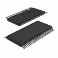
SC28L202A1DGG/G:11 NXP Semiconductors, SC28L202A1DGG/G:11 Datasheet - Page 42

SC28L202A1DGG/G:11
Manufacturer Part Number
SC28L202A1DGG/G:11
Description
IC UART DUAL W/FIFO 56-TSSOP
Manufacturer
NXP Semiconductors
Series
IMPACTr
Datasheet
1.SC28L202A1DGG118.pdf
(77 pages)
Specifications of SC28L202A1DGG/G:11
Features
False-start Bit Detection
Number Of Channels
2, DUART
Fifo's
256 Byte
Voltage - Supply
3.3V, 5V
With Parallel Port
Yes
With Auto Flow Control
Yes
With False Start Bit Detection
Yes
With Modem Control
Yes
With Cmos
Yes
Mounting Type
Surface Mount
Package / Case
56-TFSOP (0.240", 6.10mm Width)
Lead Free Status / RoHS Status
Lead free / RoHS Compliant
Other names
935279792112
SC28L202A1DGG/G
SC28L202A1DGG/G
SC28L202A1DGG/G
SC28L202A1DGG/G
Philips Semiconductors
BCRBRK – Bidding Control Register – Break Change, A and B
This register provides the 8 MSBs of the Interrupt Arbitration number for a break change interrupt.
BCRCOS – Bidding Control Register – Change of State, A and B
This register provides the 8 MSBs of the Interrupt Arbitration number for a Change of State, COS, interrupt.
BCRx – Bidding Control Register – Xon/Xoff, A and B
This register provides the 8 MSBs of the Interrupt Arbitration number for a Xon/Xoff interrupt.
BCRA – Bidding Control Register – Address, A and B
This register provides the 8 MSBs of the Interrupt Arbitration number for an address recognition event interrupt.
BCR C/T – Bidding Control Register –C/T, 0 and 1
This register provides the 8 MSBs of the Interrupt Arbitration number for a counter/timer event interrupt.
BCRLBE – Bidding Control Register – Received Loop Back Error
This register provides the 8 MSBs of the Interrupt Arbitration number for the received loop back error interrupt.
Registers of the I/O ports
IPCRL – Input Port Change Register Lower Nibble, A and B (n = A for A, n = B for B)
This register may be read to determine the current logical level of the I/O pins and examine the output of the change detectors assigned to each
pin. If the change detection is not enabled or if the pin is configured as an output, the associated change field will read b’0.
IPCRU – Input Port Change Register Upper Nibble, A and B (n = A for A, n = B for B)
This register may be read to determine the current logical level of the I/O pins and examine the output of the change detectors assigned to each
pin. If the change detection is not enabled or if the pin is configured as an output, the associated change field will read b’0.
IPR – Input Port Register, A and B (n = A for A, n = B for B)
2005 Nov 01
Bit 7
change
0 = no change
1 = change
Bit 7
0 = no change
1 = change
Bits 7:0
Logical levels of I/O(7:0)n
I/O3 n
I/O7 n change
Dual UART
Bits 7:0
MSBs of break change interrupt bid
Bits 7:0
MSBs of Change of state detectors (COS) interrupt bid
Bits 7:0
MSBs of an Xon/Xoff interrupt bid
Bits 7:0
MSBs of an address recognition event interrupt bid
Bits 7:0
MSBs of a counter/timer event interrupt bid
Bits 7:0
MSBs of a received loop back error event interrupt bid
Bit 6
change
0 = no change
1 = change
Bit 6
0 = no change
1 = change
I/O2 n
I/O6 n change
Bit 7
change
0 = no change
1 = change
Bit 7
0 = no change
1 = change
I/O1 n
I/O5 n change
Bit 6
change
0 = no change
1 = change
Bit 6
0 = no change
1 = change
I/O0 n
I/O4 n change
36
Bit 3
I/O3 n state
Reads the actual logic level at the pin.
1 = high level; 0 = low level
Bit 3
I/O7 n state
Reads the actual logic level at the pin.
1 = high level; 0 = low level
Bit 2
I/0n6 state
Bit 2
I/O2 n state
Bit 1
I/O5 n state
Bit 1
I/O1 n state
SC28L202
Product data sheet
Bit 0
I/O4 n state
Bit 0
I/O0 n
state


