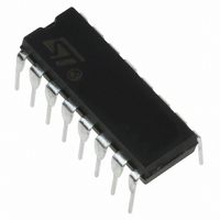
TDA1905 STMicroelectronics, TDA1905 Datasheet - Page 11

TDA1905
Manufacturer Part Number
TDA1905
Description
IC AMP AUDIO 5.5W MONO AB 16DIP
Manufacturer
STMicroelectronics
Type
Class ABr
Datasheet
1.TDA1905.pdf
(14 pages)
Specifications of TDA1905
Output Type
1-Channel (Mono)
Max Output Power X Channels @ Load
5.5W x 1 @ 8 Ohm
Voltage - Supply
4 V ~ 30 V
Features
Depop, Mute, Thermal Protection
Mounting Type
Through Hole
Package / Case
16-DIP (0.300", 7.62mm)
Amplifier Class
AB
No. Of Channels
1
Output Power
5W
Supply Voltage Range
4V To 30V
Thd + N
0.1% @ 1.5W, 4ohm, VS=9V
Load Impedance
4ohm
Operating Temperature Range
-40°C To +150°C
Rohs Compliant
Yes
Lead Free Status / RoHS Status
Lead free / RoHS Compliant
Other names
497-2160-5
Available stocks
Company
Part Number
Manufacturer
Quantity
Price
Part Number:
TDA1905
Manufacturer:
ST
Quantity:
20 000
APPLICATION SUGGESTION
The recommended values of the external components are those shown on the application circuit of fig. 21.
When the supply voltage V
in order to obtain the maximum output power.
Different values can be used. The following table can help the designer.
Component
R
g
R
R
R
R
C
C
C
C
C
C
C
C
C
P
+ R
2
3
4
5
1
1
2
3
4
5
6
7
8
9
1
Raccom.
1000 F Output DC decoupling.
0.22 F
0.22 F
2.2 F
0.1 F
value
10K
10K
100
100
20K
10 F
47 F
1K
Input signal imped. for
muting operation
Feedback resistors
Frequency stability
Increase of the output
swing with low supply
voltage.
Volume potentiometer Increase of the
Input DC
decoupling.
Inverting input DC
decoupling.
Supply voltage
bypass.
Ripple rejection
Bootstrap.
Frequency stability.
s
is less than 10V, a 100 resistor must be connected between pin 2 and pin 3
Purpose
Increase of the
attenuation in muting-on
condition. Decrease of
the input sensitivity.
Increase of gain.
Decrease of gain.
Danger of oscillation at
high frequencies with
inductive loads.
switch-on noise.
Higher cost
lower noise.
Increase of the switch-
on noise.
Increase of SVR
increase of the
switch-on time
recommended value
Larger than
Decrease of the attenu-
ation in muting on
condition.
Decrease of gain.
Increase quiescent
current.
Increase of gain.
Decrease of the input
impedance and of the
input level.
Higher low
frequency cutoff.
Higher noise.
Higher low frequency
cutoff.
Danger of
oscillations.
Degradation of SVR
Increase of the
distortion at low
frequency.
Danger of oscillation.
Higher low frequency
cutoff.
recommended value
Smaller than
Allowed range
10K
0.1 F
2.2 F 100 F
10 F
Min.
9 R
47
TDA1905
3
100K
100 F
Max.
1K
330
11/14


