TDA1558Q/N1,112 NXP Semiconductors, TDA1558Q/N1,112 Datasheet - Page 4
TDA1558Q/N1,112
Manufacturer Part Number
TDA1558Q/N1,112
Description
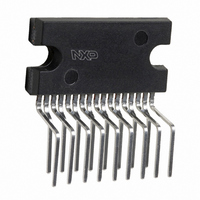
IC AMP AUDIO PWR 22W STER 17SIL
Manufacturer
NXP Semiconductors
Type
Class Br
Datasheet
1.TDA1558QN1112.pdf
(11 pages)
Specifications of TDA1558Q/N1,112
Package / Case
17-SIL (Bent and Staggered Leads)
Output Type
2-Channel (Stereo) or 4-Channel (Quad)
Max Output Power X Channels @ Load
22W x 2 @ 4 Ohm; 11W x 4 @ 2 Ohm
Voltage - Supply
6 V ~ 18 V
Features
Depop, Mute, Short-Circuit and Thermal Protection, Standby
Mounting Type
Through Hole
Product
General Purpose Audio Amplifiers
Mounting Style
SMD/SMT
Operational Class
Class-B
Audio Amplifier Function
Speaker
Total Harmonic Distortion
0.1@4Ohm@1W%
Single Supply Voltage (typ)
14.4V
Dual Supply Voltage (typ)
Not RequiredV
Power Supply Requirement
Single
Power Dissipation
60W
Rail/rail I/o Type
No
Single Supply Voltage (min)
6V
Single Supply Voltage (max)
18V
Dual Supply Voltage (min)
Not RequiredV
Dual Supply Voltage (max)
Not RequiredV
Mounting
Through Hole
Pin Count
17
Lead Free Status / RoHS Status
Lead free / RoHS Compliant
Lead Free Status / RoHS Status
Lead free / RoHS Compliant, Lead free / RoHS Compliant
Other names
568-3508-5
935043920112
TDA1558QU
935043920112
TDA1558QU


Philips Semiconductors
PINNING
FUNCTIONAL DESCRIPTION
The TDA1558Q contains four identical amplifiers with
differential input stages (two inverting and two
non-inverting), and can be used for single-ended or BTL
applications. The gain of each amplifier is fixed at 40 dB
(46 dB in BTL). Special features of this device are:
a. mute/stand-by switch
b. the harmonic distortion at low frequencies can be
decreased by connecting two diodes at pin 15 to ground or
a zener diode of 1.5 V.
May 1992
INV2
GND
SVRR
V
OUT1
GND1
OUT2
n.c.
OUT4
GND2
OUT3
V
M/SS
V
INV3
SYMBOL
INV1
INV4
P1
P2
ref
2 x 22 W or 4 x 11 W single-ended car
radio power amplifier
low stand-by current (< 100 A)
low mute/stand-by switching current (low cost supply
switch)
mute facility.
PIN
10
11
12
13
14
15
16
17
1
2
3
4
5
6
7
8
9
non-inverting input 1
inverting input 2
ground (signal)
supply voltage ripple rejection
supply voltage
output 1
power ground 1
output 2
not connected
output 4
power ground 2
output 3
supply voltage
mute/stand-by switch
internal reference voltage
inverting input 3
non-inverting input 4
DESCRIPTION
4
handbook, halfpage
– INV1
– INV4
M / SS
SVRR
GND1
GND2
OUT1
OUT2
OUT4
OUT3
INV2
GND
INV3
Fig.2 Pin configuration.
V
V
V
n.c.
P1
P2
ref
16
17
10
11
12
13
14
15
1
2
3
4
5
6
7
8
9
TDA1558Q
MCD325 - 1
Product specification
TDA1558Q
Related parts for TDA1558Q/N1,112
Image
Part Number
Description
Manufacturer
Datasheet
Request
R

Part Number:
Description:
2 X 22 W Or 4 X 11 W Single-ended Car Radio Power Amplifier
Manufacturer:
NXP Semiconductors
Datasheet:
Part Number:
Description:
Audio Amplifiers POWER AMPLIFIER
Manufacturer:
NXP Semiconductors
Datasheet:
Part Number:
Description:
NXP Semiconductors designed the LPC2420/2460 microcontroller around a 16-bit/32-bitARM7TDMI-S CPU core with real-time debug interfaces that include both JTAG andembedded trace
Manufacturer:
NXP Semiconductors
Datasheet:

Part Number:
Description:
NXP Semiconductors designed the LPC2458 microcontroller around a 16-bit/32-bitARM7TDMI-S CPU core with real-time debug interfaces that include both JTAG andembedded trace
Manufacturer:
NXP Semiconductors
Datasheet:
Part Number:
Description:
NXP Semiconductors designed the LPC2468 microcontroller around a 16-bit/32-bitARM7TDMI-S CPU core with real-time debug interfaces that include both JTAG andembedded trace
Manufacturer:
NXP Semiconductors
Datasheet:
Part Number:
Description:
NXP Semiconductors designed the LPC2470 microcontroller, powered by theARM7TDMI-S core, to be a highly integrated microcontroller for a wide range ofapplications that require advanced communications and high quality graphic displays
Manufacturer:
NXP Semiconductors
Datasheet:
Part Number:
Description:
NXP Semiconductors designed the LPC2478 microcontroller, powered by theARM7TDMI-S core, to be a highly integrated microcontroller for a wide range ofapplications that require advanced communications and high quality graphic displays
Manufacturer:
NXP Semiconductors
Datasheet:
Part Number:
Description:
The Philips Semiconductors XA (eXtended Architecture) family of 16-bit single-chip microcontrollers is powerful enough to easily handle the requirements of high performance embedded applications, yet inexpensive enough to compete in the market for hi
Manufacturer:
NXP Semiconductors
Datasheet:
Part Number:
Description:
The XA-S3 device is a member of Philips Semiconductors? XA(eXtended Architecture) family of high performance 16-bitsingle-chip microcontrollers
Manufacturer:
NXP Semiconductors
Datasheet:

Part Number:
Description:
The NXP BlueStreak LH75401/LH75411 family consists of two low-cost 16/32-bit System-on-Chip (SoC) devices
Manufacturer:
NXP Semiconductors
Datasheet:
Part Number:
Description:
The NXP LPC3130/3131 combine an 180 MHz ARM926EJ-S CPU core, high-speed USB2
Manufacturer:
NXP Semiconductors
Datasheet:
Part Number:
Description:
The NXP LPC3141 combine a 270 MHz ARM926EJ-S CPU core, High-speed USB 2
Manufacturer:
NXP Semiconductors
Part Number:
Description:
The NXP LPC3143 combine a 270 MHz ARM926EJ-S CPU core, High-speed USB 2
Manufacturer:
NXP Semiconductors

Part Number:
Description:
The NXP LPC3152 combines an 180 MHz ARM926EJ-S CPU core, High-speed USB 2
Manufacturer:
NXP Semiconductors