TDA7375V STMicroelectronics, TDA7375V Datasheet
TDA7375V
Specifications of TDA7375V
Available stocks


Related parts for TDA7375V


TDA7375V Summary of contents
Page 1
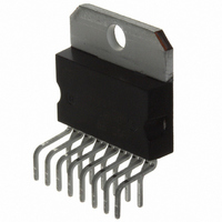
... S – SOFT SHORT AT TURN-ON – THERMAL SHUTDOWN PROXIMITY Figure 2. Block Diagram July 2008 TDA7375V Figure 1. Package MULTIWATT15 Table 1. Order Codes Part Number TDA7375V MULTIWATT 15 (Vertical) 2 PROTECTIONS: OUPUT AC/DC SHORT CIRCUIT ■ – TO GND – – ACROSS THE LOAD SOFT SHORT AT TURN-ON ■ ...
Page 2
... TDA7375V 3 DESCRIPTION The TDA7375V is a new technology class AB car radio amplifier able to work either in DUAL BRIDGE or QUAD SINGLE ENDED configuration. The exclusive fully complementary structure of the output stage and the internally fixed gain guarantees the highest possible power performances with extremely reduced component count. ...
Page 3
... Max Driving Curr. Under Fault (*) (**) (**) Sink Current at Pin 10 = 1mA = 4Ω 14.4V 4Ω 1KHz Min. Typ. Max 6 0. 3.5 90 160 TDA7375V = 25°C, amb Unit 18 V 150 mA 150 0 KΩ KΩ 0.5 dB μV μV μ μA 100 1 μ μA μA 0.7 ...
Page 4
... TDA7375V 4 STANDARD TEST AND APPLICATION CIRCUIT Figure 4. Quad Stereo Note: C9, C10, C11, C12 could be reduced if the 2W operation is not required. Figure 5. Double Bridge ST- Figure 6. Stereo/Bridge ST- BRIDGE 4/15 10K R1 ST-BY C7 10μ 0.22μ 0.22μ 0.22μ 0.22μ 47μF 10K R1 C5 10μ ...
Page 5
... Figure 7. P.C. Board and Component Layout of the fig.4 Figure 8. P.C. Board and Component Layout of the fig.5 TDA7375V 5/15 ...
Page 6
... TDA7375V Figure 9. Quiescent Drain Current vs. Supply Voltage (Single Ended and Bridge). Figure 10. Quiescent Output Voltage vs. Supply Voltage (Single Ended and Bridge). Figure 11. Output Power vs. Supply Voltage 6/15 Figure 12. Output Power vs. Supply Voltage Figure 13. OutputPower vs. Supply Voltage Figure 14. Distortion vs. Output Power ...
Page 7
... Figure 15. Distortion vs. Output Power Figure 16. Distortion vs. Output Power Figure 17. Cross-talk vs. Frequency Figure 18. Supply Voltage Rejection vs. Frequency Figure 19. Supply Voltage Rejection vs. Frequency Figure 20. Stand-by Attenuation vs. Threshold Voltage TDA7375V 7/15 ...
Page 8
... TDA7375V Figure 21. Total Power Dissipation and Efficiency vs. Output Power 5 GENERAL STRUCTURE 5.1 High Application Flexibility The availability of 4 independent channels makes it possible to accomplish several kinds of applications ranging from 4 speakers stereo (F/ speakers bridge solutions. In case of working in single ended conditions the polarity of the speakers driven by the inverting amplifier must be reversed respect to those driven by non inverting channels ...
Page 9
... BUILT-IN protectors. Additionally to the AC/DC short circuit to GND SHORT condition is signalled out during the TURN-ON PHASE so assuring correct operation for the de- of the output transistors, which is in the range of 0.3Ω (R CEsat /V is greater than unity, approximately 1+R2/R1. The DC Out In TDA7375V sat , across the speaker, a SOFT S 9/15 ) ...
Page 10
... TDA7375V vice itself and for the loudspeaker. This particular kind of protection acts in a way to avoid that the device is turned on (by ST-BY) when a resistive path (less than 16 ohms) is present between the output and GND. As the involved circuitry is nor- mally disabled when a current higher than 5mA is flowing into the ST-BY pin important, in order not to disable it, to have the external current source driving the ST-BY pin limited to 5mA ...
Page 11
... This could be done by taking into account the different timing of the diagnostic output during each case. Normally the clip detector signalling produces a low level at pin 10 that is shorter than that present under faulty conditions; based on this assumption an interface circuitry to differentiate the information is repre- sented in the schematic of fig. 29. TDA7375V 11/15 ...
Page 12
... TDA7375V Figure 28. Waveforms Figure 29. Interface circuitry to differentiate the information schematic 5.9 PCB-LAYOUT GROUNDING (general rules) The device has 2 distinct ground leads, P-GND (POWER GROUND) and S-GND (SIGNAL GROUND) which are practically disconnected from each other at chip level. Proper operation requires that P-GND and S-GND leads be connected together on the PCB-layout by means of reasonably low-resistance tracks ...
Page 13
... OUTLINE AND MECHANICAL DATA Multiwatt15 (Vertical) 0016036 J TDA7375V 13/15 ...
Page 14
... TDA7375V 7 REVISION HISTORY Table 5. Revision History Date Revision July 2004 March 2005 01-Jul-2008 14/15 2 First Issue in EDOCS 3 Changed the Style-sheet in compliance to the new “Corporate Technical Pubblications Design Guide”. Deleted package Multiwatt15 Horizontal. 4 Updated the root part number in the title of the cover page. ...
Page 15
... Australia - Belgium - Brazil - Canada - China - Czech Republic - Finland - France - Germany - Hong Kong - India - Israel - Italy - Japan - Malaysia - Malta - Morocco - Singapore - Spain - Sweden - Switzerland - United Kingdom - United States of America Please Read Carefully: © 2008 STMicroelectronics - All rights reserved STMicroelectronics group of companies www.st.com TDA7375V 15/15 ...