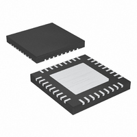
MAX9742ETX+ Maxim Integrated Products, MAX9742ETX+ Datasheet - Page 17

MAX9742ETX+
Manufacturer Part Number
MAX9742ETX+
Description
IC AMP AUDIO PWR 20.5W D 36TQFN
Manufacturer
Maxim Integrated Products
Type
Class Dr
Datasheet
1.MAX9742ETX.pdf
(36 pages)
Specifications of MAX9742ETX+
Output Type
2-Channel (Stereo)
Max Output Power X Channels @ Load
20.5W x 2 @ 8 Ohm
Voltage - Supply
20 V ~ 40 V, ±10 V ~ 20 V
Features
Depop, Differential Inputs, Mute, Short-Circuit and Thermal Protection, Shutdown
Mounting Type
Surface Mount
Package / Case
36-TQFN Exposed Pad
Product
Class-D
Output Power
16 W
Thd Plus Noise
0.08 %
Supply Current
15 mA
Maximum Power Dissipation
2.86 W
Maximum Operating Temperature
+ 85 C
Mounting Style
SMD/SMT
Audio Load Resistance
4 Ohms
Minimum Operating Temperature
- 40 C
Lead Free Status / RoHS Status
Lead free / RoHS Compliant
to-peak output voltage that causes 10% THD+N for a
given load.
where P
THD+N, R
peak-to-peak output voltage. Determine the voltage
gain (A
on the maximum peak-to-peak input voltage (V
Set the closed-loop voltage gain of the MAX9742 less
than or equal to A
unless audible clipping is acceptable for the application.
The external feedback networks of the MAX9742 input
amplifiers allow custom gain settings while maximizing
dynamic range. The input amplifiers also accommodate
a variety of standard amplifier configurations including
differential input, single-ended input, and summing
amplifiers. Due to the output current limitations of the
internal input amplifiers, always select feedback resistors
(R
Diagrams ) with values greater than or equal to 400kΩ. To
preserve gain accuracy, avoid using feedback resistors
with values greater than 1MΩ. For proper operation, limit
common-mode input voltages to ±3V.
The Typical Application Circuits/Functional Diagrams
show each channel of the MAX9742 configured as dif-
ferential input amplifiers. A differential input offers
improved noise immunity over a single-ended input. In
systems that include high-speed digital circuitry, high-
frequency noise can couple into the amplifier’s input
traces. The signals appear at the amplifier’s inputs as
common-mode noise. A differential input amplifier
amplifies the difference of the two inputs, and signals
common to both inputs are subtracted out. When con-
figured for differential inputs, the voltage gain of the
MAX9742 is set by:
where A
should be equal to R
R
F2
F1
.
, see the Typical Application Circuits/Functional
V
V
OUT_P P
OUT_10%
) necessary to attain this output voltage based
V
L
is the desired voltage gain in V/V. R
is the load resistance, and V
−
Class D Amplifier with Differential Inputs
A
=
is the output power that causes 10%
______________________________________________________________________________________
V
V
2 2 P
A
to prevent clipping of the output,
=
IN2
V
Differential Input Configuration
V
(
=
, and R
OUT_P P
V
OUT_10%
IN_P P
R
R
IN1
F1
−
−
F1
( / )
V V
( / )
V V
should be equal to
Input Amplifier
×
Single-/Dual-Supply, Stereo 16W,
R
L
OUT_P-P
)
( ) V
IN_P-P
is the
IN1
):
When using the differential input configuration, the
common-mode rejection ratio (CMRR) is primarily limit-
ed by the external resistor tolerances. Ideally, to
achieve the highest possible CMRR, the resistors
should be perfectly matched and the following condi-
tion should be met:
To ensure the MAX9742 input amplifiers operate as
fully differential integrators, connect a capacitor
between IN_+ and MID whose value is equal to C
the Feedback Capacitor (CFB_) section).
Each channel of the MAX9742 can be configured as a
single-ended input amplifier by connecting IN_+ to MID
(through an external resistor, R
the input source (see Figure 5). In this configuration,
the MAX9742 is configured as a single-ended amplifier
whose voltage gain is equal to:
where A
To minimize output offset voltages due to input bias cur-
rents, connect a resistor, R
IN_+ and MID. Select the value of R
resistances looking out of inputs of the amplifier (IN_+
and IN_-) are equal. For example, when using the dual-
supply configuration with a DC-coupled input source, the
value of R
Figure 5. Single-Ended Input Configuration
V
IN
V
OS
C
is the desired voltage gain in V/V.
IN
should be equal to R
R
R
OS
IN
A
MID
V
R
= −
R
IN1
F1
IN_-
IN_+
R
R
=
IN
OS
F
R
R
C
, (see Figure 5) between
( / )
R
FB_
IN2
OS
F2
V V
F
F
MAX9742
) and driving IN_- with
||R
Single-Ended Input
IN
OS
.
so that the DC
FB_
TO CLASS D
MODULATOR
OUT_
F
(see
17


