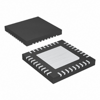
MAX9742ETX+ Maxim Integrated Products, MAX9742ETX+ Datasheet - Page 2

MAX9742ETX+
Manufacturer Part Number
MAX9742ETX+
Description
IC AMP AUDIO PWR 20.5W D 36TQFN
Manufacturer
Maxim Integrated Products
Type
Class Dr
Datasheet
1.MAX9742ETX.pdf
(36 pages)
Specifications of MAX9742ETX+
Output Type
2-Channel (Stereo)
Max Output Power X Channels @ Load
20.5W x 2 @ 8 Ohm
Voltage - Supply
20 V ~ 40 V, ±10 V ~ 20 V
Features
Depop, Differential Inputs, Mute, Short-Circuit and Thermal Protection, Shutdown
Mounting Type
Surface Mount
Package / Case
36-TQFN Exposed Pad
Product
Class-D
Output Power
16 W
Thd Plus Noise
0.08 %
Supply Current
15 mA
Maximum Power Dissipation
2.86 W
Maximum Operating Temperature
+ 85 C
Mounting Style
SMD/SMT
Audio Load Resistance
4 Ohms
Minimum Operating Temperature
- 40 C
Lead Free Status / RoHS Status
Lead free / RoHS Compliant
ABSOLUTE MAXIMUM RATINGS
V
MID, LGND, LV
MID, LGND, LV
REGLS to V
MID to REGP, REGM...............(V
REGP to REGM.......................................................-0.3V to +12V
LV
SHDN to LGND.........................................................-0.3V to +4V
SFT to LGND ............................................................-0.3V to +6V
FB_, IN_+, IN_-, REFCUR to REGP,
BOOTR to OUTR ....................................................-0.3V to +12V
BOOTL to OUTL .....................................................-0.3V to +12V
OUTR, OUTL Shorted to LGND..................................Continuous
Single-/Dual-Supply, Stereo 16W,
Class D Amplifier with Differential Inputs
Note 1: Actual power capabilities are dependent on PCB layout. See the Thermal Considerations section.
Stresses beyond those listed under “Absolute Maximum Ratings” may cause permanent damage to the device. These are stress ratings only, and functional
operation of the device at these or any other conditions beyond those indicated in the operational sections of the specifications is not implied. Exposure to
absolute maximum rating conditions for extended periods may affect device reliability.
ELECTRICAL CHARACTERISTICS—Single-Supply, Single-Ended Output
(V
10kΩ, C
R
T
2
Supply Voltage Range
Supply Current
Mute Mode Supply Current
Shutdown Current
Switching Frequency
Power-Supply Rejection Ratio
(Note 4)
Crosstalk
(Notes 5 and 6)
Continuous Output Power
(Notes 5, 6, and 7)
Efficiency
(Notes 5, 6, and 7)
DD
A
F1A
DD
OUTL to V
OUTL to V
REGM..................................(V
DD
= +25°C.) (Note 2)
_______________________________________________________________________________________
to V
= 24V, V
= 121kΩ, R
to LGND ..........................................................-0.3V to +6V
SS
SFT
PARAMETER
, NSENSE ..............................................-0.3V to +45V
SS
SS
DD
= 0.47µF, C
.........................................................-0.3V to +12V
SS
DD
DD
.......................................................-0.3V to +45V
.......................................................-45V to +0.3V
F1B
= V
, REGM, REGP, OUTR,
, REGM, REGP, OUTR,
SUB
= 562kΩ, R
OUT
= LGND = 0V, V
= 1000µF, C
REGM
REGM
F2
SYMBOL
= 681kΩ, R
PSRR
P
V
f
I
SW
OUT
DD
DD
- 0.3V) to (V
- 0.3V) to (V
SHDN
FB_1
(Note 3)
No load, output filter removed
No load, V
No load, V
V
L to R, R to L, R
R
R
V
R
R
REF
DD
DD
L
L
L
L
= 150pF, C
= 3.3V, V
= 8Ω, f
= 8Ω, f
= 4Ω, f
= 8Ω, P
REGP
REGP
= 24V + 500mV
= 35V
= 68kΩ, R
+ 0.3V)
+ 0.3V)
IN
IN
IN
SFT
SHDN
OUT
MID
= 1kHz, THD+N = 10%
= 1kHz, THD+N = 10%,
= 1kHz, THD+N = 10%
= 0V (outputs not switching)
FB_2
= 9.5W, THD+N = 10%
L
L
= 0V
= 12V, C
= 8Ω, P
= ∞, T
CONDITIONS
= 10pF, C
P-P
, f = 1kHz
Continuous Power Dissipation (T
Junction-to-Ambient Thermal Resistance (θ
Junction-to-Case Thermal Resistance (θ
Operating Temperature Range ...........................-40°C to +85°C
Maximum Junction Temperature .....................................+150°C
Storage Temperature Range .............................-65°C to +150°C
Lead Temperature (soldering, 10s) .................................+300°C
A
OUT
VDD
= T
Single-Layer Board:
36-Pin TQFN (derate 26.3mW/°C above +70°C) ...........2.11W
Multilayer Board:
36-Pin TQFN (derate 35.7mW/°C above +70°C) ...........2.86W
Single-Layer Board:
36-Pin TQFN.................................................................38°C/W
Multilayer Board:
36-Pin TQFN.................................................................28°C/W
MIN
= 1W, f = 1kHz
= 660µF, C
BOOT
to T
= 0.1µF, C
MAX
, unless otherwise noted. Typical values are at
MID1
= 10µF, C
REGP
= C
MIN
20
A
MID2
= +70°C) (Note 1)
REGM
= 10µF, R1 = R2 = R3 =
TYP
20.5
300
-78
JC
0.8
9.5
15
68
16
92
= 1µF, R
8
) ...................1.4°C/W
JA
)
MAX
1.3
40
IN_
= 30.1kΩ,
UNITS
kHz
mA
mA
mA
dB
dB
W
%
V


