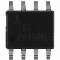
HA9P5020-5Z Intersil, HA9P5020-5Z Datasheet - Page 11

HA9P5020-5Z
Manufacturer Part Number
HA9P5020-5Z
Description
IC AMP VIDEO 100MHZ CFB 8-SOIC
Manufacturer
Intersil
Datasheet
1.HA9P5020-5Z.pdf
(23 pages)
Specifications of HA9P5020-5Z
Applications
Current Feedback
Number Of Circuits
1
-3db Bandwidth
100MHz
Slew Rate
1100 V/µs
Current - Supply
7.5mA
Current - Output / Channel
31.7mA
Voltage - Supply, Single/dual (±)
±4.5 V ~ 18 V
Mounting Type
Surface Mount
Package / Case
8-SOIC (0.154", 3.90mm Width)
Lead Free Status / RoHS Status
Lead free / RoHS Compliant
Available stocks
Company
Part Number
Manufacturer
Quantity
Price
Company:
Part Number:
HA9P5020-5Z
Manufacturer:
Intersil
Quantity:
1 684
Part Number:
HA9P5020-5Z
Manufacturer:
INTERSIL
Quantity:
20 000
Referring to Figure 7, it can be seen that R
resistor to +V
where the enable/disable function is not required on all circuits
some circuits can be permanently enabled by letting the
DISABLE pin float. If a driver is used to set the enable/disable
level, be sure that the driver does not sink more than 20µA
when the DISABLE pin is at a high level. TTL gates, especially
CMOS versions, do not violate this criteria so it is permissible to
control the enable/disable function with TTL.
Typical Applications
Two Channel Video Multiplexer
Referring to the amplifier U
cable in its characteristic impedance of 75Ω, and R
terminates the cable in its characteristic impedance. The
amplifier is set up in a gain configuration of +2 to yield an
overall network gain of +1 when driving a double terminated
cable. The value of R
gain is desired. R
inhibiting the amplifier until the switch, S
position 1. At position 1 the switch pulls the disable pin up to
the plus supply rail thereby enabling the amplifier. Since all
of the actual signal switching takes place within the amplifier,
it’s differential gain and phase parameters, which are 0.03%
and 0.03° respectively, determine the circuit’s performance.
The other circuit, U
When the plus supply rail is 5V the disable pin can be driven
by a dedicated TTL gate as discussed earlier. If a multiplexer
IC or its equivalent is used to select channels its logic must be
break before make. When these conditions are satisfied the
HA-5020 is often used as a remote video multiplexer, and the
multiplexer may be extended by adding more amplifier ICs.
Low Impedance Multiplexer
Two common problems surface when you try to multiplex
multiple high speed signals into a low impedance source
VIDEO INPUT #1
VIDEO INPUT #2
CC
R
75
R
75
if the DISABLE pin is left open. In those cases
1
6
5
holds the disable pin at ground thus
1B
3
, operates in a similar manner.
681
681
can be changed if a different network
R
R
3
8
1A
+
U
U
-
11
1B
1A
681
681
in Figure 8, R
R
R
2
7
FIGURE 8. TWO CHANNEL HIGH IMPEDANCE MULTIPLEXER
R
75
R
75
R
2000
R
2000
1
9
6
4
5
10
, is thrown to
will act as a pull-up
1
terminates the
4
back
OFF
ALL
3
2
1
HA-5020
S
1
VIDEO OUTPUT
TO 75Ω LOAD
R
100
11
such as an A/D converter. The first problem is the low source
impedance which tends to make amplifiers oscillate and
causes gain errors. The second problem is the multiplexer
which supplies no gain, introduces all kinds of distortion and
limits the frequency response. Using op amps which have an
enable/disable function, such as the HA-5020, eliminates the
multiplexer problems because the external mux chip is not
needed, and the HA-5020 can drive low impedance (large
capacitance) loads if a series isolation resistor is used.
Referring to Figure 9, both inputs are terminated in their
characteristic impedance; 75Ω is typical for video
applications. Since the drivers usually are terminated in their
characteristic impedance the input gain is 0.5, thus the
amplifiers, U
gain equal to one. Resistors R
amplifier gain, and if a different gain is desired R
changed according to the equation G = (1 + R
the frequency response of the amplifier so you should refer
to the manufacturers data sheet before changing its value.
R
circuit which configures U
prevent both amplifiers from being active simultaneously. If
this design is extended to more channels the drive logic
must be designed to be break before make. R
in the feedback loop of the amplifier so that the large open
loop amplifier gain of U
closed loop output impedance while keeping the amplifier
stable for all values of load capacitance.
The circuit shown in Figure 9 was tested for the full range of
capacitor values with no oscillations being observed; thus,
problem one has been solved. The frequency and gain
characteristics of the circuit are now those of the amplifier
and independent of any multiplexing action; thus, problem
two has been solved. The multiplexer transition time is
approximately 15µs with the component values shown.
5
, C
+5V
1
and D
NOTES:
21. U
22. All resistors in Ω.
23. S
24. Use ground plane.
2
1
, are configured in a gain of +2 to set the circuit
are an asymmetrical charge/discharge time
1
1
is break before make.
is HA-5020.
2
+5V IN
will present the load with a small
1
-5V IN
as a break before make switch to
0.1µF
0.1µF
2
and R
3
determine the
+
10µF
+
10µF
3
4
/R
is enclosed
+5V
2
-5V
2
should be
). R
June 5, 2006
FN2845.11
3
sets


