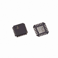
EL4543ILZ Intersil, EL4543ILZ Datasheet - Page 13

EL4543ILZ
Manufacturer Part Number
EL4543ILZ
Description
IC DRIVER TWISTED 350MHZ 20QFN
Manufacturer
Intersil
Datasheet
1.EL4543IUZ.pdf
(18 pages)
Specifications of EL4543ILZ
Applications
Driver
Output Type
Differential
Number Of Circuits
3
-3db Bandwidth
350MHz
Slew Rate
1000 V/µs
Current - Supply
14.5mA
Current - Output / Channel
60mA
Voltage - Supply, Single/dual (±)
5 V ~ 12 V, ±2.5 V ~ 6 V
Mounting Type
Surface Mount
Package / Case
20-VQFN Exposed Pad, 20-HVQFN, 20-SQFN, 20-DHVQFN
Rohs Compliant
YES
Lead Free Status / RoHS Status
Lead free / RoHS Compliant
Available stocks
Company
Part Number
Manufacturer
Quantity
Price
Company:
Part Number:
EL4543ILZ
Manufacturer:
Intersil
Quantity:
2 195
Part Number:
EL4543ILZ
Manufacturer:
INTERSIL
Quantity:
20 000
Part Number:
EL4543ILZ-T13
Manufacturer:
INTERSIL
Quantity:
20 000
Disable and Power Down
The EL4543 provides an enable disable function which
powers down, logic input high, in 900ns and powers up, logic
input low, in 212ns. Disabled the amplifiers supply current is
reduced to 1.8mA (Positive Supply) and 0mA (Negative
Supply). Note that Enable/Disable threshold is a linear
function of the supply voltage levels. The Enable/Disable
threshold voltage level is compatible with standard
TTL/CMOS and referenced to the lowest supply potential.
Proper Layout Technique
A critical concern with any PCB layout is the establishment
of a “healthy” ground plane. It is imperative to provide
ground planes terminated close to inputs to minimize input
capacitance. Additionally, the ground plane can be
selectively removed from inputs to prevent load and supply
currents from flowing near the input nodes.
In general the following guidelines apply to all PCB layout:
• Keep all traces as short as possible.
• Keep power supply bypass components as close to the
• Create a healthy ground with low impedance and
• In high frequency applications on multi-level boards try to
• Provide extremely short loops from power pin to ground.
• If it is affordable, a ferrite bead is always of benefit to
Power Dissipation Calculation
When switching at high speeds, or driving heavy loads, the
EL4543 drive capability is ultimately limited by the rise in die
temperature brought about by internal power dissipation. For
reliable operation die temperature must be kept below T
(125°C). It is necessary to calculate the power dissipation for
a given application prior to selecting package type. Power
dissipation may be calculated:
where:
• V
• I
• ΔV
• R
• I
PD
chip as possible - extremely close.
continuous ground pathways available to all grounded
components board-wide.
keep one level of board with continuous ground plane and
minimum via cutouts - providing it is affordable.
isolate device from Power Supply noise and the rest of the
circuit from the noise of the device.
application
SMAX
LOAD
S
LD
=
O
is the total power supply to the EL4543 (from V
3
= Differential load resistance
= Maximum differential output voltage of the
×
= Load current
= Maximum quiescent supply current per channel
⎛
⎜
⎝
V
S
×
I
SMAX
+
V
S
×
ΔV
----------- -
R
13
LD
O
⎞
⎟
⎠
S
+ to V
(EQ. 1)
JMAX
S
-)
EL4543
Having obtained the application's power dissipation, the
maximum junction temperature can be calculated:
T
where:
• T
• T
• PD is the power dissipation calculated above
• θ
• Note:
See Technical Bulletin 389
(http://www.intersil.com/data/tb/TB389.pdf) for additional
QFN PCB layout information.
Application Circuit
Video Transmission Along CAT5 Cable
VGA input RGB plus sync is connected with 75Ω termination
to the inputs of the EL4543. Single-ended RGB video is
converted to differential mode signals with H
V
differential signals, respectively. The 50Ω output-terminated
EL4543 drives the differential RGB with sync encoded
common-mode to CAT5 twisted pair cables. Note this
system, without signal frequency equalization, will
satisfactorily transmit along up to 200ft of CAT5 twisted-pair.
For longer cable lengths, frequency and gain equalization to
compensate for signal degradation is recommended
(EL9110) and a delay line technology (EL9115) to adjust for
phase mismatch between signals at the receiving end.
JMAX
SYNC
application (package + PCB combination). Refer to the
Package Power Dissipation curves.
For the QFN package, the thermal pad is internally
connected to VS- and may only be grounded in
applications where a single supply is used and VS- is
returned to ground. In applications where VS- is tied to a
negative voltage the thermal pad must also be connected
to the same negative voltage.
JA
JMAX
MAX
is the thermal resistance, junction to ambient, of the
=
encoded on the common-mode of the three
is the maximum ambient operating temperature
T
is the maximum junction temperature (125°C)
MAX
+
Θ
JA
×
PD
SYNC
September 13, 2007
and
FN7325.11
(EQ. 2)


