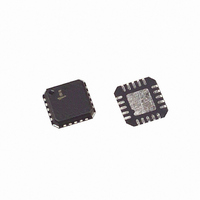
EL4543ILZ Intersil, EL4543ILZ Datasheet - Page 3

EL4543ILZ
Manufacturer Part Number
EL4543ILZ
Description
IC DRIVER TWISTED 350MHZ 20QFN
Manufacturer
Intersil
Datasheet
1.EL4543IUZ.pdf
(18 pages)
Specifications of EL4543ILZ
Applications
Driver
Output Type
Differential
Number Of Circuits
3
-3db Bandwidth
350MHz
Slew Rate
1000 V/µs
Current - Supply
14.5mA
Current - Output / Channel
60mA
Voltage - Supply, Single/dual (±)
5 V ~ 12 V, ±2.5 V ~ 6 V
Mounting Type
Surface Mount
Package / Case
20-VQFN Exposed Pad, 20-HVQFN, 20-SQFN, 20-DHVQFN
Rohs Compliant
YES
Lead Free Status / RoHS Status
Lead free / RoHS Compliant
Available stocks
Company
Part Number
Manufacturer
Quantity
Price
Company:
Part Number:
EL4543ILZ
Manufacturer:
Intersil
Quantity:
2 195
Part Number:
EL4543ILZ
Manufacturer:
INTERSIL
Quantity:
20 000
Part Number:
EL4543ILZ-T13
Manufacturer:
INTERSIL
Quantity:
20 000
Electrical Specifications
NOTE:
Absolute Maximum Ratings
Supply Voltage (V
Maximum Output Continuous Current . . . . . . . . . . . . . . . . . . ±70mA
Storage Temperature Range . . . . . . . . . . . . . . . . . .-65°C to +150°C
Operating Junction Temperature . . . . . . . . . . . . . . . . . . . . . . +135°C
CAUTION: Do not operate at or near the maximum ratings listed for extended periods of time. Exposure to such conditions may adversely impact product reliability and
result in failures not covered by warranty.
IMPORTANT NOTE: All parameters having Min/Max specifications are guaranteed. Typ values are for information purposes only. Unless otherwise noted, all tests are
at the specified temperature and are pulsed tests, therefore: T
AC PERFORMANCE
BW (-3dB)
SR
T
GBW
HD2
HD3
dP
dG
INPUT CHARACTERISTICS
V
I
Z
C
V
V
V
CMRR
EN
OUTPUT CHARACTERISTICS
I
C
DC PERFORMANCE
A
SUPPLY CHARACTERISTICS
V
I
PSRR
1. Parts are 100% tested at +25°C. Over-temperature limits established by characterization and are not production tested.
IN
OUT
S
PARAMETER
STL
IN
V
OS
DIFF
CM
N
SUPPLY
IN
OUT
S
-3dB Bandwidth
Differential Slew Rate
Settling Time to 0.1%
Gain Bandwidth Product
2nd Harmonic Distortion
3rd Harmonic Distortion
Differential Phase @ 3.58MHz
Differential Gain @ 3.58MHz
Input Referred Offset Voltage
Input Bias Current (V
Differential Input Impedance
Input Capacitance
Differential Input Range
Input Common Mode Voltage Range
Input Referred Voltage Noise
Input Common Mode Rejection Ratio
Threshold
Output Peak Current
Output Capacitance (Disabled)
Voltage Gain
Supply Operating Range
Power Supply Current (per Channel)
Power Supply Rejection Ratio
+ & V
S
-). . . . . . . . . . . . . . . . . . . . . . . . . . . .+12V
DESCRIPTION
3
V
S
(T
+ = +5V, V
IN
A
+, V
= +25°C)
IN
+)
S
- = 0V, T
J
= T
C
A
= T
= +25°C, V
V
R
f = 20MHz, R
f = 20MHz, R
Capacitance between any single input pin
and the power supplies
V
See Figure 7 for higher supply voltages.
V
Capacitance between any single output pin
and the power supplies when disabled
V
V
OUT
S
CM
IN
S
L
A
+ = +5V, V
+ to V
= 200Ω
= 0.8V
= 0 to 2V
EL4543
= 2V
S
-
IN
P-P
P-P
= 0V, R
L
L
S
- = 0V.
= 200Ω
= 200Ω
CONDITIONS
Ambient Operating Temperature . . . . . . . . . . . . . . . .-40°C to +85°C
V
V
Pb-free reflow profile . . . . . . . . . . . . . . . . . . . . . . . . . .see link below
IN
IN
http://www.intersil.com/pbfree/Pb-FreeReflow.asp
L
+, V
- - V
= 150Ω, unless otherwise specified.
INB
INB
. . . . . . . . . . . . . . . V
. . . . . . . . . . . . . . . . . . . . . . . . . . . . . . . . . . . . . . . . . .±5V
(Note 1)
MIN
1.82
12.3
600
-10
-30
60
40
70
S
0
5
- + 0.8V (min) to V
±0.75
1000
TYP
13.6
0.01
0.01
1.96
14.5
350
700
180
-70
-70
-15
1.4
27
80
60
12
80
2
4
(Note 1)
MAX
2.05
16.2
-10
2.3
September 13, 2007
S
10
12
+ - 0.8V (max)
FN7325.11
nV/√Hz
UNIT
MHz
V/µs
MHz
dBc
dBc
mV
mA
V/V
mA
µA
kΩ
pF
dB
pF
dB
ns
%
V
V
V
V
°


