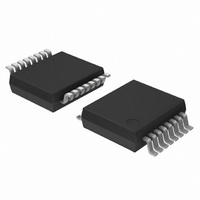
TDA9889TS/V1,518 NXP Semiconductors, TDA9889TS/V1,518 Datasheet - Page 5

TDA9889TS/V1,518
Manufacturer Part Number
TDA9889TS/V1,518
Description
IC AGC AMPLIFIER 16SSOP
Manufacturer
NXP Semiconductors
Datasheet
1.TDA9889TSV1518.pdf
(22 pages)
Specifications of TDA9889TS/V1,518
Applications
Automatic Gain Control (AGC)
Number Of Circuits
1
Current - Supply
55mA
Voltage - Supply, Single/dual (±)
4.5 V ~ 5.5 V
Mounting Type
Surface Mount
Package / Case
16-SSOP (0.200", 5.30mm Width)
Lead Free Status / RoHS Status
Lead free / RoHS Compliant
Other names
935269701518
TDA9889TSDB-T
TDA9889TSDB-T
TDA9889TSDB-T
TDA9889TSDB-T
Philips Semiconductors
PINNING
FUNCTIONAL DESCRIPTION
Figure 1 shows the simplified block diagram of the device.
The integrated circuit contains the following functional
blocks:
1. Gain controlled IF amplifier
2. Tuner AGC
3. Reference generation
4. Synthesizer for downconversion
5. Downconversion and complex filtering
6. Tracking low-pass filter with reference control
7. Low IF differential output stage
8. Logic control
9. Internal voltage stabilizer.
Gain controlled IF amplifier
The IF amplifier consists of three AC-coupled differential
stages. Gain control is performed by emitter degeneration.
Total gain control range is 70 dB (typ.). The differential
input impedance is typical 2 k in parallel with 3 pF.
2004 Nov 02
S0
REF
S2
LFS
LFLP
AGC
LIF1
LIF2
TADJ
TAGC
TAGCEXT
V
S1
GND
IF1
IF2
SYMBOL PIN
P
DVB selective AGC amplifier
10
11
12
13
14
15
16
1
2
3
4
5
6
7
8
9
logic switch S0 input (frequency
select)
4 MHz crystal or reference input
logic switch S2 input (AGC select)
loop filter synthesizer PLL
loop filter low-pass control PLL
AGC control voltage input
low IF differential output 1
low IF differential output 2
tuner AGC TakeOver Point (TOP)
adjustment
tuner AGC output
external tuner AGC voltage input
supply voltage (+5 V)
logic switch S1 input (frequency
select)
ground supply
IF differential input 1
IF differential input 2
DESCRIPTION
5
Tuner AGC
The tuner AGC is realized by a TakeOver Point (TOP)
network and a peak-level detector. The threshold level of
the peak detector can be adjusted by an external
potentiometer connected to pin TADJ. For IF signals
above this threshold the level detector provides a
discharge current to pin TAGC. An additional current
source is internally connected to this pin providing charge
current to the external tuner AGC capacitor. For IF signals
of 8 dB below the threshold voltage this current will be
increased by a factor of approximately 40 for faster AGC
reaction. The ratio of discharge to charge current is
normally approximately 2000 and approximately 50 for
fast mode.
For use of the device in different applications the charge
current can be switched off, for hybrid applications the
signal at pin TAGCEXT can be fed via a transmission gate
to pin TAGC (TDA9888TS; TDA9889TS combined with
analog IF), controlled by the 3-state input pin S2. With an
activated transmission gate all internal currents are off.
In the event that the tuner AGC is not needed (e.g. TAGC
from channel decoder or from an analog IF in hybrid
chassis), pin TADJ should be left open-circuit and
therefore all internal AGC currents will be switched off.
handbook, halfpage
LFLP
AGC
TDA9888TS; TDA9889TS
REF
LIF1
LIF2
LFS
Fig.2 Pin configuration.
S0
S2
1
2
3
4
5
6
7
8
TDA9888TS
TDA9889TS
MHC093
16
15
14
13
12
11
10
9
Product specification
IF2
IF1
GND
S1
V P
TAGCEXT
TAGC
TADJ


