BGY785A,112 NXP Semiconductors, BGY785A,112 Datasheet
BGY785A,112
Specifications of BGY785A,112


Related parts for BGY785A,112


BGY785A,112 Summary of contents
Page 1
BGY785A 750 MHz, 18.5 dB gain push-pull amplifier Rev. 6 — 29 September 2010 1. Product profile 1.1 General description Hybrid high dynamic range cascode amplifier module in a SOT115J package operating with a voltage supply (DC). ...
Page 2
... NXP Semiconductors 2. Pinning information Table 2. Pin Ordering information Table 3. Type number BGY785A 4. Limiting values Table 4. In accordance with the Absolute Maximum Rating System (IEC 60134). Symbol stg T mb BGY785A Product data sheet Pinning Description input common common +V B common common output ...
Page 3
... NXP Semiconductors 5. Characteristics Table 5. Bandwidth 40 MHz to 750 MHz ° case S L Symbol Parameter G power gain p SL slope cable equivalent FL flatness of frequency response s input return losses 11 s output return losses 22 CTB composite triple beat X cross modulation mod CSO composite second order distortion ...
Page 4
... NXP Semiconductors Table 6. Bandwidth 40 MHz to 600 MHz ° case S L Symbol Parameter G power gain p SL slope cable equivalent FL flatness of frequency response s input return losses 11 s output return losses 22 CTB composite triple beat X cross modulation mod CSO composite second order distortion d second order distortion ...
Page 5
... NXP Semiconductors Table 7. Bandwidth 40 MHz to 550 MHz ° case S L Symbol Parameter G power gain p SL slope cable equivalent FL flatness of frequency response s input return losses 11 s output return losses 22 CTB composite triple beat X cross modulation mod CSO composite second order distortion d second order distortion ...
Page 6
... NXP Semiconductors Table 8. Bandwidth 40 MHz to 450 MHz ° case S L Symbol Parameter G power gain p SL slope cable equivalent FL flatness of frequency response s input return losses 11 s output return losses 22 CTB composite triple beat X cross modulation mod CSO composite second order distortion d second order distortion ...
Page 7
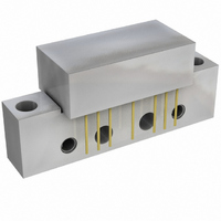
... NXP Semiconductors 6. Package outline Rectangular single-ended package; aluminium flange; 2 vertical mounting holes 6-32 UNC and 2 extra horizontal mounting holes; 7 gold-plated in-line leads DIMENSIONS (mm are the original dimensions UNIT b c max. max. max. 0.51 mm 20.8 9.5 0.25 27.2 0.38 OUTLINE VERSION IEC SOT115J Fig 1 ...
Page 8
... Modifications: The format of this data sheet has been redesigned to comply with the new identity guidelines of NXP Semiconductors. • Legal texts have been adapted to the new company name where appropriate. • Package outline drawings have been updated to the latest version. ...
Page 9
... In no event shall NXP Semiconductors be liable for any indirect, incidental, punitive, special or consequential damages (including - without limitation - lost profits, lost savings, business interruption, costs related to the removal or ...
Page 10
... NXP Semiconductors’ specifications such use shall be solely at customer’s own risk, and (c) customer fully indemnifies NXP Semiconductors for any liability, damages or failed product claims resulting from customer design and use of the product for automotive applications beyond NXP Semiconductors’ ...
Page 11
... NXP Semiconductors 10. Contents 1 Product profile . . . . . . . . . . . . . . . . . . . . . . . . . . 1 1.1 General description . . . . . . . . . . . . . . . . . . . . . 1 1.2 Features and benefits . . . . . . . . . . . . . . . . . . . . 1 1.3 Applications . . . . . . . . . . . . . . . . . . . . . . . . . . . 1 1.4 Quick reference data . . . . . . . . . . . . . . . . . . . . 1 2 Pinning information . . . . . . . . . . . . . . . . . . . . . . 2 3 Ordering information . . . . . . . . . . . . . . . . . . . . . 2 4 Limiting values Characteristics . . . . . . . . . . . . . . . . . . . . . . . . . . 3 6 Package outline . . . . . . . . . . . . . . . . . . . . . . . . . 7 7 Revision history . . . . . . . . . . . . . . . . . . . . . . . . . 8 8 Legal information 8.1 Data sheet status . . . . . . . . . . . . . . . . . . . . . . . 9 8 ...