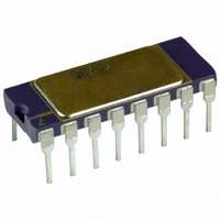
AD539JD Analog Devices Inc, AD539JD Datasheet - Page 10

AD539JD
Manufacturer Part Number
AD539JD
Description
IC MULT/DIV DUAL CH LIN 16-CDIP
Manufacturer
Analog Devices Inc
Specifications of AD539JD
Rohs Status
RoHS non-compliant
Function
Analog Multiplier/Divider
Number Of Bits/stages
2
Package / Case
16-CDIP (0.300", 7.62mm)
Number Of Elements
2
Output Type
Single
Power Supply Requirement
Dual
Single Supply Voltage (typ)
Not RequiredV
Single Supply Voltage (min)
Not RequiredV
Single Supply Voltage (max)
Not RequiredV
Dual Supply Voltage (typ)
±5/±9/±12V
Dual Supply Voltage (min)
±4.5V
Dual Supply Voltage (max)
±15V
Operating Temperature Classification
Commercial
Mounting
Through Hole
Pin Count
16
Package Type
SBCDIP
Lead Free Status / RoHS Status
Not Compliant
Available stocks
Company
Part Number
Manufacturer
Quantity
Price
Part Number:
AD539JD
Manufacturer:
ADI/亚德诺
Quantity:
20 000
THEORY OF OPERATION
CIRCUIT DESCRIPTION
Figure 18 shows a simplified schematic of the AD539. Q1 to Q6
are large-geometry transistors designed for low distortion and
low noise. Emitter-area scaling further reduces distortion: Q1 is
three times larger than Q2; Q4 and Q5 are each three times
larger than Q3 and Q6 and are twice as large as Q1 and Q2. A
stable reference current of I
band gap reference circuit and applied to the common emitter
node of a controlled cascode formed by Q1 and Q2. When V
0 V, all of I
control amplifier, which lowers the voltage on the base of Q2.
As V
balance the control current, V
V
Q5 are at ground potential and the bases of Q2, Q3, and Q6 are
commoned, all three controlled cascodes divide the current
applied to their emitter nodes in the same proportion. The
control loop is stabilized by the external capacitor, C
The signal voltages, V
are first converted to currents by voltage-to-current converters
with a g
becomes a current of ±1.15 mA, which is superimposed on a
bias of 2.75 mA and applied to the common emitter node of
controlled cascode Q3/Q4 or Q5/Q6. As previously explained,
the proportion of this current steered to the output node is
linearly dependent on V
inputs, a signal of ±1 mA (0.873 × ±1.15 mA) and a bias
component of 2.4 mA (0.873 × 2.75 mA) appear at the output.
The bias component absorbed by the 1.25 kΩ resistors also
connected to V
to an external load resistor (in which case scaling is not
accurate) or can be forced into either or both of the 6 kΩ
feedback resistors (to the Z and W nodes) by an external op
amp. In the latter case, scaling accuracy is guaranteed.
AD539
X
(3 V) this fraction is 0.873. Because the base of Q1, Q4, and
X
is raised, the fraction of I
m
of 575 μmhos. Thus, the full-scale input of ±2 V
REF
flows in Q1 due to the action of the high gain
X
and the resulting signal current can be applied
BASE COMMON
Y1
0V TO +3V FS
and V
X
. Therefore, for full-scale V
REF
+V
–V
X
Y2
= 1.375 mA is produced by a
V
/2.5 kΩ. At the full-scale value of
REF
X
S
S
(generically referred to as V
13
Figure 18. Simplified Schematic of AD539 Multiplier (16-Lead SBDIP and PDIP Shown)
1
4
5
flowing in Q2 is forced to
1.375mA
1.2mA FS
I
REF
GENERATOR
REFERENCE
BAND-GAP
Q1
=
Q2
2.5kΩ
HF COMP
C
X
.
and V
CONTROL
AMPLIFIER
±2V FS
V
Y1
Y
2
Y
Rev. B | Page 10 of 20
X
),
OUTPUT
C
3nF MIN
3
=
CHAN1
C
(EXT)
±1mA FS
14
Q3
GENERAL RECOMMENDATIONS
The AD539 is a high speed circuit and requires considerable
care to achieve its full performance potential. A high quality
ground plane should be used with the device either soldered
directly into the board or mounted in a low profile socket. In
Figure 18, an open triangle denotes a direct, short connection
to this ground plane; the BASE COMMON pins (Pin 12 and
Pin 13) are especially prone to unwanted signal pickup. Power
supply decoupling capacitors of 0.1 μF to 1 μF should be
connected from the +V
ground plane. In applications using external high speed op
amps, use separate supply decoupling. It is good practice to
insert small (10 Ω) resistors between the primary supply and
the decoupling capacitor.
The control amplifier compensation capacitor, C
likewise have short leads to ground and a minimum value of
3 nF. Unless maximum control bandwidth is essential, it is
advisable to use a larger value of 0.01 μF to 0.1 μF to improve
the signal channel phase response, high frequency crosstalk,
and high frequency distortion. The control bandwidth is
inversely proportional to this capacitance, typically 2 MHz for C
0.01 μF, V
control channel can be improved by using a feedforward
capacitor of 5% to 20% the value of C
HF COMP pins (Pin 1 and Pin 2). Optimum transient response
results when the rise/fall time of V
control channel response time.
V
gain is zero for V
(see Figure 18) causing control feedthrough. Recovery time
from negative values of V
signal Schottky diode with its cathode connected to HF COMP
(Pin 2) and its anode grounded. This constrains the voltage
swing on C
maximum value, but any overdrive appears as control
feedthrough at the output.
1.25kΩ
6kΩ
6kΩ
X
should not exceed the specified range of 0 V to 3 V. The ac
Q4
INPUT COMMON
16
15
W1
Z1
X
12
7
= 1.7 V. The bandwidth and pulse response of the
C
W2
. Above V
Z2
10
9
Q5
X
6kΩ
6kΩ
< 0 V but there remains a feedforward path
Q6
X
S
1.25kΩ
= 3.2 V, the ac gain limits at its
±1mA FS
and −V
X
can be improved by adding a small
S
11
8
6
pins (Pin 4 and Pin 5) to the
X
CHAN2
OUTPUT
OUTPUT
COMMON
V
±2V FS
Y2
are commensurate with the
C
between the V
C
, should
X
and
C
=


