AD539JD Analog Devices Inc, AD539JD Datasheet - Page 6
AD539JD
Manufacturer Part Number
AD539JD
Description
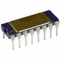
IC MULT/DIV DUAL CH LIN 16-CDIP
Manufacturer
Analog Devices Inc
Specifications of AD539JD
Rohs Status
RoHS non-compliant
Function
Analog Multiplier/Divider
Number Of Bits/stages
2
Package / Case
16-CDIP (0.300", 7.62mm)
Number Of Elements
2
Output Type
Single
Power Supply Requirement
Dual
Single Supply Voltage (typ)
Not RequiredV
Single Supply Voltage (min)
Not RequiredV
Single Supply Voltage (max)
Not RequiredV
Dual Supply Voltage (typ)
±5/±9/±12V
Dual Supply Voltage (min)
±4.5V
Dual Supply Voltage (max)
±15V
Operating Temperature Classification
Commercial
Mounting
Through Hole
Pin Count
16
Package Type
SBCDIP
Lead Free Status / RoHS Status
Not Compliant
Available stocks
Company
Part Number
Manufacturer
Quantity
Price

Part Number:
AD539JD
Manufacturer:
ADI/亚德诺
Quantity:
20 000


Table 3. 16-Lead PDIP and SBDIP Pin Function Descriptions
Pin No.
1
2
3
4
5
6
7
8
9
10
11
12
13
14
15
16
AD539
Mnemonic
V
HF COMP
V
+V
–V
V
INPUT COMMON
OUTPUT COMMON
W2
Z2
CHAN2 OUTPUT
BASE COMMON
BASE COMMON
CHAN1 OUTPUT
Z1
W1
X
Y1
Y2
S
S
Figure 3. 16-Lead PDIP and SBDIP Pin Configurations (N-16, D-16)
Description
Control Channel Input.
High Frequency Compensation.
Channel 1 Input.
Positive Supply Rail.
Negative Supply Rail.
Channel 2 Input.
Internal Common Connection for the Input Amplifier Circuitry.
Internal Common Connection for The Output Amplifier Circuitry.
6 kΩ Feedback Resistor for Channel 2.
6 kΩ Feedback Resistor for Channel 2.
Channel 2 Product of V
Increases Negative Output Compliance.
Increases Negative Output Compliance.
Channel 1 Product of V
6 kΩ Feedback Resistor for Channel 1.
6 kΩ Feedback Resistor for Channel 1.
OUTPUT COMMON
INPUT COMMON
HF COMP
+V
–V
V
V
V
Y1
Y2
X
S
S
Rev. B | Page 6 of 20
1
2
3
4
5
6
7
8
(Not to Scale)
TOP VIEW
X
X
AD539
and V
and V
Y2
Y1
.
.
16
15
14
13
12
11
10
9
W1
Z1
CHAN1 OUTPUT
BASE COMMON
BASE COMMON
CHAN2 PUTPUT
Z2
W2
Related parts for AD539JD
Image
Part Number
Description
Manufacturer
Datasheet
Request
R

Part Number:
Description:
±1.7g Dual-Axis IMEMS Accelerometer Evaluation Board
Manufacturer:
Analog Devices Inc
Datasheet:

Part Number:
Description:
Inertial Sensor Evaluation System
Manufacturer:
Analog Devices Inc
Datasheet:
Part Number:
Description:
Manufacturer:
Analog Devices Inc
Datasheet:
Part Number:
Description:
Manufacturer:
Analog Devices Inc
Datasheet:
Part Number:
Description:
Manufacturer:
Analog Devices Inc
Datasheet:
Part Number:
Description:
Manufacturer:
Analog Devices Inc
Datasheet:
Part Number:
Description:
Manufacturer:
Analog Devices Inc
Datasheet:
Part Number:
Description:
Manufacturer:
Analog Devices Inc
Datasheet:
Part Number:
Description:
Manufacturer:
Analog Devices Inc
Datasheet:
Part Number:
Description:
Manufacturer:
Analog Devices Inc
Datasheet:
Part Number:
Description:
Manufacturer:
Analog Devices Inc
Datasheet:
Part Number:
Description:
Manufacturer:
Analog Devices Inc
Datasheet:
Part Number:
Description:
Manufacturer:
Analog Devices Inc
Datasheet: