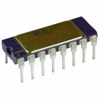
AD539JD Analog Devices Inc, AD539JD Datasheet - Page 3

AD539JD
Manufacturer Part Number
AD539JD
Description
IC MULT/DIV DUAL CH LIN 16-CDIP
Manufacturer
Analog Devices Inc
Specifications of AD539JD
Rohs Status
RoHS non-compliant
Function
Analog Multiplier/Divider
Number Of Bits/stages
2
Package / Case
16-CDIP (0.300", 7.62mm)
Number Of Elements
2
Output Type
Single
Power Supply Requirement
Dual
Single Supply Voltage (typ)
Not RequiredV
Single Supply Voltage (min)
Not RequiredV
Single Supply Voltage (max)
Not RequiredV
Dual Supply Voltage (typ)
±5/±9/±12V
Dual Supply Voltage (min)
±4.5V
Dual Supply Voltage (max)
±15V
Operating Temperature Classification
Commercial
Mounting
Through Hole
Pin Count
16
Package Type
SBCDIP
Lead Free Status / RoHS Status
Not Compliant
Available stocks
Company
Part Number
Manufacturer
Quantity
Price
Part Number:
AD539JD
Manufacturer:
ADI/亚德诺
Quantity:
20 000
SPECIFICATIONS
T
guaranteed.
Table 1.
Parameter
SIGNAL CHANNEL DYNAMICS
CONTROL CHANNEL DYNAMICS
SIGNAL INPUTS, V AND V
A
Minimal Configuration
Standard 2-Channel Multiplier
Wideband 2-Channel Multiplier
Wideband Single-Channel VCA
Bandwidth, −3 dB
Nominal Full-Scale Input
Operational Range, Degraded
Input Resistance
Bias Current
Offset Voltage
Power Supply Sensitivity
= 25°C, V
Bandwidth, −3 dB
Maximum Output
Feedthrough
Differential Phase Linearity
Group Delay
Maximum Output
Feedthrough, f < 100 kHz
Crosstalk (Channel 1 to
RTO Noise, 10 Hz to 1 MHz
THD + Noise
Bandwidth, −3 dB (LH0032)
Maximum Output V
Feedthrough V
Performance
T
MIN
f < 1 MHz
f = 20 MHz
−1 V < V
−2 V < V
Channel 2)
V
V
Bandwidth, −3 dB
Maximum Output
Feedthrough
X
Y
to T
= 1 V
= 3 V
MAX
S
= ±5 V, unless otherwise specified. V
Y
Y
dc < +1 V
dc < +2 V
Y1
X
= 0 V
X
Y2
= 3 V
Test Conditions/Comments
See Figure 22
R
0.1 V < V
V
f = 3.58 MHz, V
V
f = 3.58 MHz, V
V
V
f = 1 MHz
See Figure 20
V
V
V
V
V
f = 10 kHz, V
f = 10 kHz, V
See Figure 20
0.1 V < V
V
V
V
See Figure 24
0.1 V < V
V ac = 1 V rms
75 Ω load
V
C
V
−V
V
V
L
Y
Y
Y
Y
Y
Y
X
X
X
X
Y1
X
X
X
C
X
X
X
= 50 Ω, C
ac = 100 mV
ac = 100 mV
= 0 V, V
ac = 1 V rms
ac = 1.5 V rms, f = 3 MHz
ac = 1.0 V rms, f = 3 MHz
= 0 V, V
= 3 V, V
= 3 V, V
= 3 V, f < 100 kHz
= 1.5 V, V
= −0.01 V, f = 5 MHz
ac = 100 mV rms
= 3 V, V
= 3 V, V
= 3000 pF, V
S
= 1 V rms, V
≤ 7 V
X
X
X
< 3 V, V
Y
Y
< 3 V,
< 3 V,
Y
Y
Y
Y
ac = 1.5 V rms
ac = 1.5 V rms
ac = 1.5 V rms
ac = 1 V rms,
= 0 V
= 0 V
C
Y
Y
Y
= 0.01 μF
= 0 V
ac = 1 V rms
ac = 1 V rms
X
X
Y2
X
= 3 V,
= 3 V,
Y
dc = 1.5 V,
= 0 V,
ac = 1 V rms
Y
= V
Y1
− V
Rev. B | Page 3 of 20
Y2
Min
30
±4.2
, V
X
1
= V
AD539J
Typ
60
−10
−75
−55
±0.2
±0.5
4
4.5
1
−40
200
0.02
0.04
25
4.5
14
50
±1
−54
5
±2
400
10
5
10
2
X1
– V
X2
. All minimum and maximum specifications are
Max
30
20
1
1
Min
30
±4.2
1
AD539K
Typ
60
−10
−75
−55
±0.2
±0.5
4
4.5
1
−40
200
0.02
0.04
25
4.5
14
50
±1
−54
5
±2
400
10
5
5
2
Max
20
10
1
1
Min
30
±4.2
1
AD539S
Typ
60
−10
−75
−55
±0.2
±0.5
4
4.5
1
−40
200
0.02
0.04
25
4.5
14
50
±1
−54
5
±2
400
10
5
15
2
Max
30
20
35
1
1
AD539
Unit
MHz
dBm
dBm
dBm
Degrees
Degrees
ns
V
mV rms
dB
nV/√Hz
%
%
MHz
V rms
mV rms
MHz
V
dB
MHz
V
V
kΩ
μA
mV
mV
mV/V


