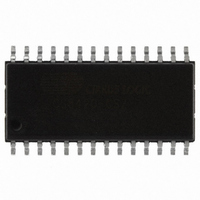
CS8420-CSZ Cirrus Logic Inc, CS8420-CSZ Datasheet - Page 37

CS8420-CSZ
Manufacturer Part Number
CS8420-CSZ
Description
IC SAMPLE RATE CONVERTER 28SOIC
Manufacturer
Cirrus Logic Inc
Type
Sample Rate Converterr
Specifications of CS8420-CSZ
Package / Case
28-SOIC
Applications
CD-R, DAT, DVD, MD, VTR
Mounting Type
Surface Mount
Operating Supply Voltage
5 V
Operating Temperature Range
- 10 C to + 70 C
Mounting Style
SMD/SMT
Resolution
17 bit to 24 bit
Control Interface
3 Wire, Serial
Supply Voltage Range
4.75V To 5.25V
Audio Ic Case Style
SOIC
No. Of Pins
28
Bandwidth
20kHz
Rohs Compliant
Yes
Audio Control Type
Volume
Dc
0841
Lead Free Status / RoHS Status
Lead free / RoHS Compliant
For Use With
598-1782 - EVALUATION BOARD FOR CS8420
Lead Free Status / Rohs Status
Lead free / RoHS Compliant
Other names
598-1125-5
Available stocks
Company
Part Number
Manufacturer
Quantity
Price
Company:
Part Number:
CS8420-CSZ
Manufacturer:
CIRRUS
Quantity:
319
Company:
Part Number:
CS8420-CSZ
Manufacturer:
CIRRUS
Quantity:
9 908
Part Number:
CS8420-CSZ
Manufacturer:
CIRRUS
Quantity:
20 000
Company:
Part Number:
CS8420-CSZ/D1
Manufacturer:
CIRRUS
Quantity:
378
Company:
Part Number:
CS8420-CSZR
Manufacturer:
NICHICON
Quantity:
4 200
DS245F4
10.5
RUN
CLK[1:0]
OUTC
INC
RXD[1:0]
7
0
Clock Source Control (04h)
RUN
This register configures the clock sources of various blocks. In conjunction with the Data Flow
Control register, various Receiver/Transmitter/Transceiver modes may be selected.
0 - Internal clocks are stopped. Internal state machines are reset. The fully static
control port is operational, allowing registers to be read or changed. Reading and
writing the U and C data buffers is not possible. Power consumption is low (default).
1 - Normal part operation. This bit must be written to the 1 state to allow the CS8420
to begin operation. All input clocks should be stable in frequency and phase when
RUN is set to 1.
Output side master clock input (OMCK) frequency to output sample rate (Fso) ratio selector. If
these bits are changed during normal operation, then always stop the CS8420 first (RUN = 0),
then write the new value, then start the CS8420 (RUN = 1).
00 - OMCK frequency is 256*Fso(default)
01 - OMCK frequency is 384*Fso
10 - OMCK frequency is 512*Fso
11 - reserved
0 - OMCK input pin (modified by the selected divide ratio bits CLK1 & CLK0,
(default)
1 - Recovered Input Clock
0 - Recovered Input Clock (default)
1 - OMCK input pin (modified by the selected divide ratio bits CLK1 & CLK0)
Recovered Input Clock Source
00 - 256*Fsi, where Fsi is derived from the ILRCK pin (only possible when the
serial audio input port is in Slave mode, default)
01 - 256*Fsi, where Fsi is derived from the AES3 input frame rate
10 - Bypass the PLL and apply an external 256*Fsi clock via the RMCK pin. The AES3
receiver is held in synchronous reset. This setting is useful to prevent UNLOCK
interrupts when using an external RMCK and inputting data via the serial audio
input port.
11 - Reserved
The RUN bit controls the internal clocks, allowing the CS8420 to be placed in a
Output Time Base
Input Time Base Clock Source
“powered down”, low current consumption, state.
6
CLK1
5
CLK0
4
OUTC
3
INC
2
RXD1
1
CS8420
RXD0
0
37


