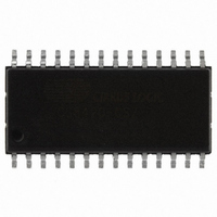
CS8420-CSZ Cirrus Logic Inc, CS8420-CSZ Datasheet - Page 56

CS8420-CSZ
Manufacturer Part Number
CS8420-CSZ
Description
IC SAMPLE RATE CONVERTER 28SOIC
Manufacturer
Cirrus Logic Inc
Type
Sample Rate Converterr
Specifications of CS8420-CSZ
Package / Case
28-SOIC
Applications
CD-R, DAT, DVD, MD, VTR
Mounting Type
Surface Mount
Operating Supply Voltage
5 V
Operating Temperature Range
- 10 C to + 70 C
Mounting Style
SMD/SMT
Resolution
17 bit to 24 bit
Control Interface
3 Wire, Serial
Supply Voltage Range
4.75V To 5.25V
Audio Ic Case Style
SOIC
No. Of Pins
28
Bandwidth
20kHz
Rohs Compliant
Yes
Audio Control Type
Volume
Dc
0841
Lead Free Status / RoHS Status
Lead free / RoHS Compliant
For Use With
598-1782 - EVALUATION BOARD FOR CS8420
Lead Free Status / Rohs Status
Lead free / RoHS Compliant
Other names
598-1125-5
Available stocks
Company
Part Number
Manufacturer
Quantity
Price
Company:
Part Number:
CS8420-CSZ
Manufacturer:
CIRRUS
Quantity:
319
Company:
Part Number:
CS8420-CSZ
Manufacturer:
CIRRUS
Quantity:
9 908
Part Number:
CS8420-CSZ
Manufacturer:
CIRRUS
Quantity:
20 000
Company:
Part Number:
CS8420-CSZ/D1
Manufacturer:
CIRRUS
Quantity:
378
Company:
Part Number:
CS8420-CSZR
Manufacturer:
NICHICON
Quantity:
4 200
56
13.2
SDOUT
LO
HI
-
-
-
-
-
-
Hardware Mode 1 Description (DEFAULT Data Flow, AES3 Input)
Hardware Mode 1 data flow is shown in
verted. The audio data at the new rate is then output both via the serial audio output port and via the AES3
transmitter.
The channel status data, user data and validity bit information are handled in four alternative modes: 1A and
1B, determined by a start-up resistor on the COPY pin. In mode 1A, the received PRO, COPY, ORIG, EM-
PH, and AUDIO channel status bits are output on pins. The transmitted channel status bits are copied from
the received channel status data, and the transmitted U and V bits are 0.
In mode 1B, only the COPY and ORIG pins are output, and reflect the received channel status data. The
transmitted channel status bits, user data and validity bits are input serially via the PRO/C, EMPH/U and
AUDIO/V pins.
Start-up options are shown in
choice of four serial audio output port formats, and the source for transmitted C, U and V data. The following
pages contain the detailed pin descriptions for Hardware mode 1.
If a validity, parity, bi-phase, or lock receiver error occurs, the current audio sample will be held.
RMCK
LO
LO
HI
HI
-
-
-
-
RXP
RXN
Figure 20
RERR
RMCK
Power supply pins (VD+, VA+, DGND, AGND), the reset pin (RST) and the PLL filter pin (FILT)
are omitted from this diagram. Please refer to the Typical Connection Diagram for hook-up details.
LO
LO
HI
HI
Figure 24. Hardware Mode 1 - Default Data Flow, AES3 Input
-
-
-
-
AES3 Rx
&
Decoder
DFC0
shows the timing requirements.
RERR
COPY
Table 8. Hardware Mode 1 Start-Up Options
LO
Table
HI
-
-
MUTE
DFC1
Clocked by
Input Derived Clock
8, and allow choice of the serial audio output port as a master or slave,
Serial Output Port is Slave
Serial Output Port is Master
Mode1A: C transmitted data is copied from received data, U & V = 0,
received PRO, EMPH, AUDIO are visible.
Mode 1B: CUV transmitted data is input serially on pins, received PRO,
EMPH, AUDIO are not visible
Serial Output Format OF1
Serial Output Format OF2
Serial Output Format OF3
Serial Output Format OF4
PRO/C
Figure
S/AES
COPY ORIG EMPH/U
Sample
Rate
Converter
VD+
24. Audio data is input via the AES3 receiver, and rate con-
C & U bit Data Buffer
Clocked by
Output Clock
H/S
AUDIO/V TCBL
Output
Clock
Source
Function
AES3
Encoder
& Tx
Serial
Audio
Output
OMCK
TXP
TXN
TCBLD
OLRCK
OSCLK
SDOUT
CS8420
DS245F4


