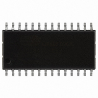
CS8420-CSZ Cirrus Logic Inc, CS8420-CSZ Datasheet - Page 39

CS8420-CSZ
Manufacturer Part Number
CS8420-CSZ
Description
IC SAMPLE RATE CONVERTER 28SOIC
Manufacturer
Cirrus Logic Inc
Type
Sample Rate Converterr
Specifications of CS8420-CSZ
Package / Case
28-SOIC
Applications
CD-R, DAT, DVD, MD, VTR
Mounting Type
Surface Mount
Operating Supply Voltage
5 V
Operating Temperature Range
- 10 C to + 70 C
Mounting Style
SMD/SMT
Resolution
17 bit to 24 bit
Control Interface
3 Wire, Serial
Supply Voltage Range
4.75V To 5.25V
Audio Ic Case Style
SOIC
No. Of Pins
28
Bandwidth
20kHz
Rohs Compliant
Yes
Audio Control Type
Volume
Dc
0841
Lead Free Status / RoHS Status
Lead free / RoHS Compliant
For Use With
598-1782 - EVALUATION BOARD FOR CS8420
Lead Free Status / Rohs Status
Lead free / RoHS Compliant
Other names
598-1125-5
Available stocks
Company
Part Number
Manufacturer
Quantity
Price
Company:
Part Number:
CS8420-CSZ
Manufacturer:
CIRRUS
Quantity:
319
Company:
Part Number:
CS8420-CSZ
Manufacturer:
CIRRUS
Quantity:
9 908
Part Number:
CS8420-CSZ
Manufacturer:
CIRRUS
Quantity:
20 000
Company:
Part Number:
CS8420-CSZ/D1
Manufacturer:
CIRRUS
Quantity:
378
Company:
Part Number:
CS8420-CSZR
Manufacturer:
NICHICON
Quantity:
4 200
DS245F4
10.7
SOMS
SOSF
SORES[1:0]
SOJUST
SODEL
SOSPOL
SOLRPOL
SOMS
7
Serial Audio Output Port Data Format (06h)
SOSF
0 - Serial audio output port is in Slave mode (default)
1 - Serial audio output port is in Master mode
OSCLK frequency (for Master mode)
0 - 64*Fso (default)
1 - 128*Fso
set as the source
00 - 24 bit resolution (default)
01 - 20 bit resolution
10 - 16 bit resolution
11 - Direct copy of the received NRZ data from the AES3 receiver (including C, U, and
V bits, the time slot normally occupied by the P bit is used to indicate the location
of the block start, SDOUT pin only, serial audio output port clock must be derived
from the AES3 receiver recovered clock)
0 - Left-Justified (default)
1 - Right-Justified (Master mode only)
0 - MSB of SDOUT data occurs in the first OSCLK period after the OLRCK edge
1 - MSB of SDOUT data occurs in the second OSCLK period after the OLRCK edge
0 - SDOUT transitions occur on falling edges of OSCLK (default)
1 - SDOUT transitions occur on rising edges of OSCLK
OLRCK clock polarity
0 - SDOUT data is for the left channel when OLRCK is high (default)
1 - SDOUT data is for the right channel when OLRCK is high
Master/Slave Mode Selector
Resolution of the output data on SDOUT and AES3 output when the sample rate converter is
Justification of SDOUT data relative to OLRCK
Delay of SDOUT data relative to OLRCK, for left-justified data formats
OSCLK clock polarity
6
(default)
SORES1
5
SORES0
4
SOJUST
3
SODEL
2
SOSPOL
1
SOLRPOL
CS8420
0
39


