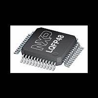
LPC11U23FBD48 NXP Semiconductors, LPC11U23FBD48 Datasheet - Page 9

LPC11U23FBD48
Manufacturer Part Number
LPC11U23FBD48
Description
The LPC11U23FBD48 is a ARM Cortex-M0 based, low-cost 32-bit MCU, designed for 8/16-bit microcontroller applications, offering performance, low power, simple instruction set and memory addressing together with reduced code size compared to existing 8/
Manufacturer
NXP Semiconductors
Datasheet
1.LPC11U23FBD48.pdf
(70 pages)
Available stocks
Company
Part Number
Manufacturer
Quantity
Price
Company:
Part Number:
LPC11U23FBD48/301,
Manufacturer:
Intersil
Quantity:
71
Company:
Part Number:
LPC11U23FBD48/301,
Manufacturer:
NXP Semiconductors
Quantity:
10 000
NXP Semiconductors
Table 3.
LPC11U2X
Product data sheet
Symbol
RESET/PIO0_0
PIO0_1/CLKOUT/
CT32B0_MAT2/
USB_FTOGGLE
PIO0_2/SSEL0/
CT16B0_CAP0
PIO0_3/USB_VBUS
PIO0_4/SCL
PIO0_5/SDA
Pin description
6.2 Pin description
Table 3
port number. The default function after reset is listed first. All port pins have internal
pull-up resistors enabled after reset except for the true open-drain pins PIO0_4 and
PIO0_5.
Every port pin has a corresponding IOCON register for programming the digital or analog
function, the pull-up/pull-down configuration, the repeater, and the open-drain modes.
The USART, counter/timer, and SSP functions are available on more than one port pin.
9
2
3
8
10
11
shows all pins and their assigned digital or analog functions in order of the GPIO
C1
C2
F1
H2
G3 15
H3
3
4
10
14
16
All information provided in this document is subject to legal disclaimers.
4
5
13
19
20
21
[2]
[3]
[3]
[3]
[4]
[4]
Rev. 2 — 13 January 2012
Reset
state
[1]
I; PU
-
I; PU
-
-
-
I; PU
-
-
I; PU
-
I; IA
-
I; IA
-
Type Description
I
I/O
I/O
O
O
O
I/O
I/O
I
I/O
I
I/O
I/O
I/O
I/O
RESET — External reset input with 20 ns glitch filter.
A LOW-going pulse as short as 50 ns on this pin
resets the device, causing I/O ports and peripherals to
take on their default states, and processor execution
to begin at address 0. This pin also serves as the
debug select input. LOW level selects the JTAG
boundary scan. HIGH level selects the ARM SWD
debug mode.
PIO0_0 — General purpose digital input/output pin.
PIO0_1 — General purpose digital input/output pin. A
LOW level on this pin during reset starts the ISP
command handler or the USB device enumeration.
CLKOUT — Clockout pin.
CT32B0_MAT2 — Match output 2 for 32-bit timer 0.
USB_FTOGGLE — USB 1 ms Start-of-Frame signal.
PIO0_2 — General purpose digital input/output pin.
SSEL0 — Slave select for SSP0.
CT16B0_CAP0 — Capture input 0 for 16-bit timer 0.
PIO0_3 — General purpose digital input/output pin. A
LOW level on this pin during reset starts the ISP
command handler. A HIGH level during reset starts
the USB device enumeration.
USB_VBUS — Monitors the presence of USB bus
power.
PIO0_4 — General purpose digital input/output pin
(open-drain).
SCL — I
High-current sink only if I
selected in the I/O configuration register.
PIO0_5 — General purpose digital input/output pin
(open-drain).
SDA — I
High-current sink only if I
selected in the I/O configuration register.
2
2
32-bit ARM Cortex-M0 microcontroller
C-bus clock input/output (open-drain).
C-bus data input/output (open-drain).
2
2
C Fast-mode Plus is
C Fast-mode Plus is
LPC11U2x
© NXP B.V. 2012. All rights reserved.
9 of 70


