EL9115ILZ-T13 Intersil, EL9115ILZ-T13 Datasheet - Page 3
EL9115ILZ-T13
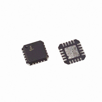
Manufacturer Part Number
EL9115ILZ-T13
Description
IC ANALOG DELAY LINE TRPL 20-QFN
Manufacturer
Intersil
Type
Video Delay Liner
Datasheet
1.EL9115ILZ-T13.pdf
(9 pages)
Specifications of EL9115ILZ-T13
Applications
Analog Beamforming, Skew Control
Mounting Type
Surface Mount
Package / Case
20-VQFN Exposed Pad, 20-HVQFN, 20-SQFN, 20-DHVQFN
Lead Free Status / RoHS Status
Lead free / RoHS Compliant


AC Electrical Specifications
NOTES:
Pin Descriptions
BW -3dB
BW 0.1dB
SR
t
V
Glitch
THD
X
V
d
t
D
t
t
t_en_ck
1. All supply currents measured with Delay R = 0ns, G = mid delay, B = full delay.
2. Delay increment limits are derived by taking Maximum Delay limits and dividing by the number of steps for the device (e.g. the number of steps
R
MAX
PD
MAX
PARAMETER
t
OVER
t
N
ELDT
- t
for the EL9115 is 31).
F
PIN NUMBER
10
12
13
14
15
16
17
18
11
1
2
3
4
5
6
7
8
9
3dB Bandwidth
0.1dB Bandwidth
Slew Rate
Transient Response Time
Voltage Overshoot
Switching Glitch
Total Harmonic Distortion
Hostile Crosstalk
Output Noise
Nominal Delay Increment
Maximum Delay
Delay Diff Between Channels
Propagation Delay
Max s_clock Frequency
Minimum Separation Between Serial
Enable and Clock
DESCRIPTION
NSENABLE
PIN NAME
CENABLE
3
SCLOCK
TESTG
SDATA
TESTB
GNDO
VSMO
GOUT
ROUT
BOUT
VSPO
GND
VSM
VSP
GIN
RIN
BIN
V
SA
+ = V
A
+ = +5V, V
+5V for delay circuitry and input amp
Red channel input, ref GND
0V for delay circuitry supply
Green channel input, ref GND
-5V for input amp
Blue channel input, ref GND
Chip enable logical +5V enables chip
ENABLE for serial input; enable on low
Data into registers; logic threshold 1.2V
Clock to enter data; logical; data written on negative edge
Blue channel output, ref GND
-5V for output buffers
Green channel output, ref GND
0V reference for input and output buffers
Red channel output, ref GND
+5V for output buffers
Blue channel phase detector output
Green channel phase detector output
0ns Delay Time
0ns Delay Time
0ns Delay Time
20% to 80%, for all delays, 1V step
for any delay, response to 1V step input
Time for o/p to settle after last s_clock edge
1V
mid delay setting
Stimulate G, measure R/B at 1MHz
Gain X2, measured at 75Ω load
Note 2
Measured input to output
Maximum programming clock speed
Check enable low edge can occur after
t_en_ck of previous (ignored) clock and up to
before t_en_ck of next (wanted) clock. Clock
edges occurring within t_en_ck of the enable
edge will have uncertain effect.
SA
P-P
- = V
EL9115
10MHz sinewave, offset by +0.2V at
A
- = -5V, T
CONDITION
A
O
O
= +25°C, exposed die plate = -5V, unless otherwise specified.
O
PIN DESCRIPTION
1.75
MIN
55
TYP
122
400
100
2.5
-50
-80
2.5
1.6
9.8
60
62
10
5
2
MAX
2.25
-40
70
10
September 22, 2009
mV
FN7441.5
UNIT
MHz
MHz
V/µs
MHz
dB
dB
ns
ns
ns
ns
ns
ns
%
%
RMS
Related parts for EL9115ILZ-T13
Image
Part Number
Description
Manufacturer
Datasheet
Request
R

Part Number:
Description:
IC ANLG VIDEO DELAY LINE 20-QFN
Manufacturer:
Intersil
Datasheet:

Part Number:
Description:
IC ANALOG DELAY LINE TRPL 20-QFN
Manufacturer:
Intersil
Datasheet:
Part Number:
Description:
IC ANALOG DELAY LINE TRPL 20-QFN
Manufacturer:
Intersil
Datasheet:

Part Number:
Description:
Intersil Corporation [CMOS Serial Controller Interface]
Manufacturer:
Intersil Corporation
Datasheet:
Part Number:
Description:
Manufacturer:
Intersil Corporation
Datasheet:
Part Number:
Description:
357-036-542-201 CARDEDGE 36POS DL .156 BLK LOPRO
Manufacturer:
Intersil Corporation
Datasheet:
Part Number:
Description:
1024-Word x 4-Bit LSI Static RAM
Manufacturer:
Intersil Corporation
Datasheet:
Part Number:
Description:
General Purpose NPN Transistor Arrays FN341.4
Manufacturer:
Intersil Corporation
Datasheet:
Part Number:
Description:
CMOS 16-Bit Microprocessor
Manufacturer:
Intersil Corporation
Datasheet:
Part Number:
Description:
Manufacturer:
Intersil Corporation
Datasheet:
Part Number:
Description:
Manufacturer:
Intersil Corporation
Datasheet:
Part Number:
Description:
Manufacturer:
Intersil Corporation
Datasheet:
Part Number:
Description:
Manufacturer:
Intersil Corporation
Datasheet:
Part Number:
Description:
CMOS 6-Bit Latch and Decoder Memory Interfaces
Manufacturer:
Intersil Corporation
Datasheet:
Part Number:
Description:
CA3046General Purpose NPN Transistor Arrays
Manufacturer:
Intersil Corporation
Datasheet: