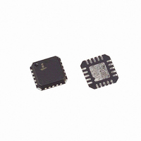
EL9115ILZ-T13 Intersil, EL9115ILZ-T13 Datasheet - Page 6

EL9115ILZ-T13
Manufacturer Part Number
EL9115ILZ-T13
Description
IC ANALOG DELAY LINE TRPL 20-QFN
Manufacturer
Intersil
Type
Video Delay Liner
Datasheet
1.EL9115ILZ-T13.pdf
(9 pages)
Specifications of EL9115ILZ-T13
Applications
Analog Beamforming, Skew Control
Mounting Type
Surface Mount
Package / Case
20-VQFN Exposed Pad, 20-HVQFN, 20-SQFN, 20-DHVQFN
Lead Free Status / RoHS Status
Lead free / RoHS Compliant
Applications Information
EL9115 is a triple analog delay line receiver that allows skew
compensation between any three high frequency signals.
This part compensates for time skew introduced by a typical
CAT-5 cable with differing electrical lengths on each pair.
The EL9115 can be independently programmed via SPI
interface in steps of 2ns up to 62ns total delay on each
channel while achieving over 80MHz bandwidth.
Figure 13 shows the EL9115 block diagram. The 3 analog
inputs are ground reference single-ended signals. After the
signal is received, the delay is introduced by switching filter
blocks into the signal path. Each filter block is an all-pass
filter introducing 2ns delay. In addition to time delay, each
filter block also introduces some low pass filtering. As a
result, the bandwidth of the signal path decreases from
120MHz at 0ns delay setting to 80MHz at the maximum
delay setting, as shown in Figure 1 of the “Typical
Performance Curves” on page 4.
In addition to delay, the extra amplifiers in the signal path
also introduce offset voltage. The output offset voltage can
shift by 100mV for X2 high setting and 50mV for X2 low.
In operation, it is best to allocate the most delayed signal
0ns delay then increase the delay on the other channels to
bring them into line. This will result in the lowest power and
distortion solution to balancing delays.
Power Dissipation
As the delay setting increases, additional filter blocks turn on
and insert into the signal path. For each 2ns of delay per
channel, V
not change significantly. Under the extreme settings, the
positive supply current reaches 140mA and the negative
SP
current increases by 0.9mA while V
6
10
2
4
6
9
8
R_IN
G_IN
B_IN
SDATA
SCLOCK
NSENABLE
3
+
+
+
5
1
FIGURE 13. EL9115 BLOCK DIAGRAM
SM
19
does
[BOTTOM PLATE]
CONTROL LOGIC
EL9115
17
DELAY LINE
DELAY LINE
DELAY LINE
C
18
supply current can be 35mA. Operating at ±5V power supply,
the total power dissipation is:
θ
calculated. This is done using Equation 2:
Where:
T
T
For a 20 Ld package in a proper layout PCB heatsinking
copper area, 40°C/W θ
achieved. To disperse the heat, the bottom heatspeader
must be soldered to the PCB. Heat flows through the
heatspreader to the circuit board copper then spreads and
convects to air. Thus, the PCB copper plane becomes the
heatsink (see TB389). This has proven to be a very effective
technique. A separate application note, which details the
20 Ld QFN PCB design considerations, is available.
PD
θ
JA
A
J
JA
is the maximum junction temperature (+135°C)
is the maximum ambient temperature (+85°C)
required for long term reliable operation can be
=
=
5 140mA
(
T
•
J
–
T
vwxyz
00000
00001
00010
00011
00100
00101
00110
A
16
12
) PD
⁄
TABLE 1. SERIAL BUS DATA
+
+
+
+
5 35mA
CENABLE 7
•
14
=
R_OUT
G_OUT
B_OUT
57°
JA
X2
C W
thermal resistance can be
⁄
=
15
13
11
20
875mW
DELAY
10
12
0
2
4
6
8
September 22, 2009
FN7441.5
(EQ. 1)
(EQ. 2)


