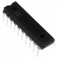
M74HCT541B1R STMicroelectronics, M74HCT541B1R Datasheet - Page 2

M74HCT541B1R
Manufacturer Part Number
M74HCT541B1R
Description
IC BUFF/DVR TRI-ST 8BIT 20DIP
Manufacturer
STMicroelectronics
Series
74HCTr
Datasheet
1.M74HCT541RM13TR.pdf
(9 pages)
Specifications of M74HCT541B1R
Logic Type
Buffer/Line Driver, Non-Inverting
Number Of Elements
1
Number Of Bits Per Element
8
Current - Output High, Low
6mA, 6mA
Voltage - Supply
4.5 V ~ 5.5 V
Operating Temperature
-55°C ~ 125°C
Mounting Type
Through Hole
Package / Case
20-DIP (0.300", 7.62mm)
Logic Family
HCT
Number Of Channels Per Chip
8
Polarity
Non-Inverting
Supply Voltage (max)
5.5 V
Supply Voltage (min)
4.5 V
Maximum Operating Temperature
+ 125 C
Mounting Style
Through Hole
High Level Output Current
- 6 mA
Low Level Output Current
6 mA
Maximum Power Dissipation
500 mW
Minimum Operating Temperature
- 55 C
Number Of Lines (input / Output)
8 / 3
Output Type
3-State
Propagation Delay Time
28 ns at 4.5 V
Logic Device Type
Buffer, Non Inverting
Supply Voltage Range
4.5V To 5.5V
Logic Case Style
DIP
No. Of Pins
20
Operating Temperature Range
-55°C To +125°C
Family Type
HCT
Rohs Compliant
Yes
Lead Free Status / RoHS Status
Lead free / RoHS Compliant
Other names
497-1916-5
M74HCT541
INPUT AND OUTPUT EQUIVALENT CIRCUIT
TRUTH TABLE
X : Don’t Care
Z : High Impedance
ABSOLUTE MAXIMUM RATINGS
Absolute Maximum Ratings are those values beyond which damage to the device may occur. Functional operation under these conditions is
not implied
(*) 500mW at 65 C; derate to 300mW by 10mW/ C from 65 C to 85 C
RECOMMENDED OPERATING CONDITIONS
2/9
I
CC
Symbol
Symbol
V
V
T
t
I
or I
T
V
P
V
I
T
r
V
OK
I
V
stg
, t
CC
IK
O
CC
op
O
D
O
L
I
I
f
GND
G1
Supply Voltage
DC Input Voltage
DC Output Voltage
DC Input Diode Current
DC Output Diode Current
DC Output Current
DC V
Power Dissipation
Storage Temperature
Lead Temperature (10 sec)
Supply Voltage
Input Voltage
Output Voltage
Operating Temperature
Input Rise and Fall Time (V
H
X
L
L
CC
or Ground Current
Parameter
Parameter
INPUT
CC
G2
X
H
L
L
= 4.5 to 5.5V)
PIN DESCRIPTION
2, 3, 4, 5, 6,
18, 17, 16,
15, 14, 13,
PIN No
7, 8, 9
12, 11
1, 19
10
20
An
X
X
H
L
SYMBOL
A1 to A8
Y1 to Y8
G1, G2
GND
V
CC
-0.5 to V
-0.5 to V
-65 to +150
-55 to 125
-0.5 to +7
4.5 to 5.5
0 to V
0 to V
0 to 500
500(*)
Value
Value
Output Enable Inputs
Data Inputs
Bus Outputs
Ground (0V)
Positive Supply Voltage
300
NAME AND FUNCTION
20
20
35
70
CC
CC
CC
CC
+ 0.5
+ 0.5
OUTPUT
Yn
H
Z
Z
L
Unit
Unit
mW
mA
mA
mA
mA
°C
°C
°C
ns
V
V
V
V
V
V


