MC74HC244ADWG ON Semiconductor, MC74HC244ADWG Datasheet - Page 4
MC74HC244ADWG
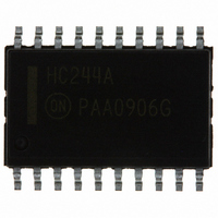
Manufacturer Part Number
MC74HC244ADWG
Description
IC BUFF/DVR TRI-ST DUAL 20SOIC
Manufacturer
ON Semiconductor
Series
74HCr
Specifications of MC74HC244ADWG
Logic Type
Buffer/Line Driver, Non-Inverting
Number Of Elements
2
Number Of Bits Per Element
4
Current - Output High, Low
7.8mA, 7.8mA
Voltage - Supply
2 V ~ 6 V
Operating Temperature
-55°C ~ 125°C
Mounting Type
Surface Mount
Package / Case
20-SOIC (7.5mm Width)
Circuit Type
Low-Power Schottky
Current, Supply
160 μA
Function Type
8-Channels
Logic Function
Buffer/Driver/Receiver
Number Of Circuits
Octal
Package Type
SOIC-20
Special Features
Non-Inverting, Tri-State
Temperature, Operating, Range
-55 to +125 °C
Voltage, Supply
2 to 6 V
Logic Family
HC
Logical Function
Buffer/Line Driver
Number Of Elements
2
Number Of Channels
8
Number Of Inputs
8
Number Of Outputs
8
Operating Supply Voltage (typ)
2.5/3.3/5V
Output Type
3-State
Polarity
Non-Inverting
Propagation Delay Time
165ns
High Level Output Current
-7.8mA
Low Level Output Current
7.8mA
Operating Supply Voltage (max)
6V
Operating Supply Voltage (min)
2V
Quiescent Current
4uA
Technology
CMOS
Pin Count
20
Mounting
Surface Mount
Operating Temp Range
-55C to 125C
Operating Temperature Classification
Military
Logic Device Type
Buffer, Non Inverting
Supply Voltage Range
2V To 6V
Logic Case Style
SOIC
No. Of Pins
20
Operating Temperature Range
-55°C To +125°C
Msl
MSL 3 - 168 Hours
Family Type
HC
Rohs Compliant
Yes
Lead Free Status / RoHS Status
Lead free / RoHS Compliant
Other names
MC74HC244ADWG
MC74HC244ADWGOS
MC74HC244ADWGOS
Available stocks
Company
Part Number
Manufacturer
Quantity
Price

Part Number:
MC74HC244ADWG
Manufacturer:
ON/安森美
Quantity:
20 000


NOTE: Information on typical parametric values and high frequency or heavy load considerations can be found in Chapter 2 of the ON
NOTE: For propagation delays with loads other than 50 pF, and information on typical parametric values, see Chapter 2 of the ON
* Used to determine the no−load dynamic power consumption: P
DC ELECTRICAL CHARACTERISTICS
AC ELECTRICAL CHARACTERISTICS
Symbol
Symbol
ON Semiconductor High−Speed CMOS Data Book (DL129/D).
t
t
t
t
t
t
t
C
C
V
t
PLH
TLH
I
I
PLZ
PZL
PHL
PHZ
PZH
THL
C
I
OZ
CC
OL
out
PD
in
in
,
,
,
,
Semiconductor High−Speed CMOS Data Book (DL129/D).
Semiconductor High−Speed CMOS Data Book (DL129/D).
Power Dissipation Capacitance (Per Buffer)*
Maximum Low−Level Output
Voltage
Maximum Input Leakage Current
Maximum Three−State Leakage
Current
Maximum Quiescent Supply Cur-
rent (per Package)
Maximum Propagation Delay, A to YA or B to YB
Maximum Propagation Delay, Output Enable to YA or YB
Maximum Propagation Delay, Output Enable to YA or YB
Maximum Output Transition Time, Any Output
Maximum Input Capacitance
Maximum Three−State Output Capacitance
(Figures 1 and 3)
(Figures 2 and 4)
(Figures 2 and 4)
(Figures 1 and 3)
(Output in High−Impedance State)
Parameter
Parameter
(Voltages Referenced to GND)
(C
L
V
|I
V
V
Output in High−Impedance State
V
V
V
I
= 50 pF, Input t
out
out
in
in
in
in
out
in
= V
= V
= V
= V
= V
| v 20 mA
= 0 mA
= V
IL
IL
CC
IL
CC
CC
Test Conditions
http://onsemi.com
or V
|I
|I
|I
or GND
or GND
out
out
out
or GND
IH
| v 2.4 mA
| v 6.0 mA
| v 7.8 mA
r
D
= t
= C
4
f
= 6 ns)
PD
V
CC
2
f + I
CC
V
V
V
2.0
4.5
6.0
3.0
4.5
6.0
6.0
6.0
6.0
2.0
3.0
4.5
6.0
2.0
3.0
4.5
6.0
2.0
3.0
4.5
6.0
2.0
3.0
4.5
6.0
CC
V
V
CC
CC
−
−
. For load considerations, see Chapter 2 of the
– 55 to
– 55 to
25_C
25_C
± 0.1
± 0.5
Typical @ 25°C, V
0.26
0.26
0.26
110
110
0.1
0.1
0.1
4.0
96
50
18
15
60
22
19
60
22
19
60
23
12
10
10
15
Guaranteed Limit
Guaranteed Limit
v 85_C
v85_C
± 1.0
± 5.0
0.33
0.33
0.33
115
140
140
0.1
0.1
0.1
40
60
23
20
70
28
24
70
28
24
75
27
15
13
10
15
34
CC
v 125_C
= 5.0 V
v125_C
± 1.0
± 10
160
135
165
165
0.1
0.1
0.1
0.4
0.4
0.4
70
27
23
80
33
28
80
33
28
90
32
18
15
10
15
Unit
Unit
mA
mA
mA
pF
pF
pF
ns
ns
ns
ns
V
Related parts for MC74HC244ADWG
Image
Part Number
Description
Manufacturer
Datasheet
Request
R

Part Number:
Description:
ON Semiconductor [VOLTAGE REGULATOR]
Manufacturer:
ON Semiconductor
Datasheet:
Part Number:
Description:
357-036-542-201 CARDEDGE 36POS DL .156 BLK LOPRO
Manufacturer:
ON Semiconductor
Datasheet:
Part Number:
Description:
357-036-542-201 CARDEDGE 36POS DL .156 BLK LOPRO
Manufacturer:
ON Semiconductor
Datasheet:
Part Number:
Description:
357-036-542-201 CARDEDGE 36POS DL .156 BLK LOPRO
Manufacturer:
ON Semiconductor
Datasheet:
Part Number:
Description:
357-036-542-201 CARDEDGE 36POS DL .156 BLK LOPRO
Manufacturer:
ON Semiconductor
Datasheet:
Part Number:
Description:
357-036-542-201 CARDEDGE 36POS DL .156 BLK LOPRO
Manufacturer:
ON Semiconductor
Datasheet:
Part Number:
Description:
357-036-542-201 CARDEDGE 36POS DL .156 BLK LOPRO
Manufacturer:
ON Semiconductor
Datasheet:
Part Number:
Description:
357-036-542-201 CARDEDGE 36POS DL .156 BLK LOPRO
Manufacturer:
ON Semiconductor
Datasheet:
Part Number:
Description:
357-036-542-201 CARDEDGE 36POS DL .156 BLK LOPRO
Manufacturer:
ON Semiconductor
Datasheet:
Part Number:
Description:
357-036-542-201 CARDEDGE 36POS DL .156 BLK LOPRO
Manufacturer:
ON Semiconductor
Datasheet:
Part Number:
Description:
357-036-542-201 CARDEDGE 36POS DL .156 BLK LOPRO
Manufacturer:
ON Semiconductor
Datasheet:
Part Number:
Description:
Manufacturer:
ON Semiconductor
Datasheet:
Part Number:
Description:
Manufacturer:
ON Semiconductor
Datasheet:
Part Number:
Description:
Manufacturer:
ON Semiconductor
Datasheet: