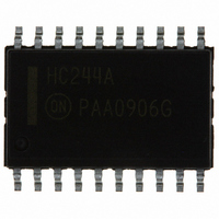
MC74HC244ADWG ON Semiconductor, MC74HC244ADWG Datasheet - Page 5

MC74HC244ADWG
Manufacturer Part Number
MC74HC244ADWG
Description
IC BUFF/DVR TRI-ST DUAL 20SOIC
Manufacturer
ON Semiconductor
Series
74HCr
Specifications of MC74HC244ADWG
Logic Type
Buffer/Line Driver, Non-Inverting
Number Of Elements
2
Number Of Bits Per Element
4
Current - Output High, Low
7.8mA, 7.8mA
Voltage - Supply
2 V ~ 6 V
Operating Temperature
-55°C ~ 125°C
Mounting Type
Surface Mount
Package / Case
20-SOIC (7.5mm Width)
Circuit Type
Low-Power Schottky
Current, Supply
160 μA
Function Type
8-Channels
Logic Function
Buffer/Driver/Receiver
Number Of Circuits
Octal
Package Type
SOIC-20
Special Features
Non-Inverting, Tri-State
Temperature, Operating, Range
-55 to +125 °C
Voltage, Supply
2 to 6 V
Logic Family
HC
Logical Function
Buffer/Line Driver
Number Of Elements
2
Number Of Channels
8
Number Of Inputs
8
Number Of Outputs
8
Operating Supply Voltage (typ)
2.5/3.3/5V
Output Type
3-State
Polarity
Non-Inverting
Propagation Delay Time
165ns
High Level Output Current
-7.8mA
Low Level Output Current
7.8mA
Operating Supply Voltage (max)
6V
Operating Supply Voltage (min)
2V
Quiescent Current
4uA
Technology
CMOS
Pin Count
20
Mounting
Surface Mount
Operating Temp Range
-55C to 125C
Operating Temperature Classification
Military
Logic Device Type
Buffer, Non Inverting
Supply Voltage Range
2V To 6V
Logic Case Style
SOIC
No. Of Pins
20
Operating Temperature Range
-55°C To +125°C
Msl
MSL 3 - 168 Hours
Family Type
HC
Rohs Compliant
Yes
Lead Free Status / RoHS Status
Lead free / RoHS Compliant
Other names
MC74HC244ADWG
MC74HC244ADWGOS
MC74HC244ADWGOS
Available stocks
Company
Part Number
Manufacturer
Quantity
Price
Part Number:
MC74HC244ADWG
Manufacturer:
ON/安森美
Quantity:
20 000
INPUTS
A1, A2, A3, A4, B1, B2, B3, B4
(Pins 2, 4, 6, 8, 11, 13, 15, 17)
form on the corresponding Y outputs, when the outputs are
enabled.
CONTROLS
Enable A, Enable B (Pins 1, 19)
to these pins, the outputs are enabled and the devices
DATA INPUT
Data input pins. Data on these pins appear in noninverted
Output enables (active−low). When a low level is applied
YA OR YB
OUTPUT
A OR B
*Includes all probe and jig capacitance
t
DEVICE
UNDER
PLH
t
TEST
r
Figure 3. Test Circuit
t
TLH
10%
10%
50%
50%
90%
90%
OUTPUT
Figure 1.
TEST POINT
C
L
*
t
f
t
PHL
SWITCHING WAVEFORMS
t
THL
V
GND
PIN DESCRIPTIONS
CC
http://onsemi.com
TEST CIRCUITS
5
OUTPUT Y
OUTPUT Y
DEVICE
UNDER
function as noninverting buffers. When a high level is
applied, the outputs assume the high impedance state.
OUTPUTS
YA1, YA2, YA3, YA4, YB1, YB2, YB3, YB4
(Pins 18, 16, 14, 12, 9, 7, 5, 3)
output−enable pins, these outputs are either noninverting
outputs or high−impedance outputs.
TEST
ENABLE
A OR B
Device outputs. Depending upon the state of the
*Includes all probe and jig capacitance
OUTPUT
50%
Figure 4. Test Circuit
TEST POINT
50%
50%
t
t
PZL
PZH
C
Figure 2.
1 kW
L
*
t
t
PHZ
PLZ
CONNECT TO V
TESTING t
CONNECT TO GND WHEN
TESTING t
10%
90%
PLZ
PHZ
AND t
AND t
CC
V
GND
HIGH
IMPEDANCE
V
V
HIGH
IMPEDANCE
CC
OL
OH
WHEN
PZL
PZH
.
.


