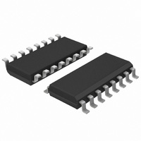
N74F367D,602 NXP Semiconductors, N74F367D,602 Datasheet - Page 6

N74F367D,602
Manufacturer Part Number
N74F367D,602
Description
IC BUFFER DVR HEX N-INV 16SOICN
Manufacturer
NXP Semiconductors
Series
74Fr
Datasheet
1.N74F367D602.pdf
(9 pages)
Specifications of N74F367D,602
Logic Type
Buffer/Line Driver, Non-Inverting
Package / Case
16-SOIC (3.9mm Width)
Number Of Elements
2
Number Of Bits Per Element
2, 4 (Hex)
Current - Output High, Low
15mA, 64mA
Voltage - Supply
4.5 V ~ 5.5 V
Operating Temperature
0°C ~ 70°C
Mounting Type
Surface Mount
Logic Family
N74F
Number Of Channels Per Chip
6
Polarity
Non-Inverting
Supply Voltage (max)
5.5 V
Supply Voltage (min)
4.5 V
Maximum Operating Temperature
70 C
Mounting Style
SMD/SMT
High Level Output Current
- 15 mA
Low Level Output Current
64 mA
Minimum Operating Temperature
0 C
Number Of Lines (input / Output)
8 / 6
Output Type
3-State
Propagation Delay Time
5 ns
Lead Free Status / RoHS Status
Lead free / RoHS Compliant
Lead Free Status / RoHS Status
Lead free / RoHS Compliant, Lead free / RoHS Compliant
Other names
568-1730-5
933756800602
N74F367D
933756800602
N74F367D
Philips Semiconductors
AC WAVEFORMS
For all waveforms, V
TEST CIRCUIT AND WAVEFORM
2004 Jan 30
Hex buffer/driver
Waveform 2. 3-State Output Enable time to HIGH level and
OE
Yn
C
SWITCH POSITION
GENERATOR
DEFINITIONS:
R
R
L
TEST
t
t
All other
T
L
PLZ
PZL
PULSE
Yn
= Load resistor;
= Load capacitance includes jig and probe capacitance;
= Termination resistance should be equal to Z
In
see AC electrical characteristics for value.
see AC electrical characteristics for value.
pulse generators.
Waveform 1. For non-inverting outputs
Test Circuit for 3-State Outputs
Output Disable time from HIGH level
V
V
M
IN
t
PZH
M
= 1.5 V
SWITCH
closed
closed
open
V
M
t
PLH
R
T
D.U.T.
V
M
V
CC
V
M
V
V
OUT
t
M
PHZ
V
M
t
PHL
C
L
R
R
SF00914
L
L
V
M
V
SF00913
OUT
OH
– 0.3 V
0 V
of
7.0 V
NEGATIVE
PULSE
POSITIVE
PULSE
6
family
74F
90%
10%
OE
amplitude
Waveform 3. 3-State Output Enable time to LOW level
Yn
3.0 V
V
INPUT PULSE REQUIREMENTS
V
M
90%
M
and Output Disable time from LOW level
10%
t
t
TLH (
THL (
Input Pulse Definition
1.5 V
V
M
V
t
M
t
t
r
f
PZL
)
)
rep. rate
1 MHz
t
t
w
w
V
M
t
t
TLH (
THL (
500 ns 2.5 ns
t
t
r
f
t
10%
90%
)
)
w
V
t
M
PLZ
V
V
M
M
t
TLH
90%
10%
74F367
2.5 ns
t
THL
V
Product data
SF00777
OL
AMP (V)
0 V
0 V
SF00915
AMP (V)
+ 0.3 V
3.5 V


