MC74HCT244ANG ON Semiconductor, MC74HCT244ANG Datasheet - Page 3
MC74HCT244ANG
Manufacturer Part Number
MC74HCT244ANG
Description
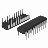
IC BUFF/DVR/RCVR 3ST DUAL 20DIP
Manufacturer
ON Semiconductor
Series
74HCTr
Specifications of MC74HCT244ANG
Logic Type
Buffer/Line Driver, Non-Inverting
Number Of Elements
2
Number Of Bits Per Element
4
Current - Output High, Low
6mA, 6mA
Voltage - Supply
4.5 V ~ 5.5 V
Operating Temperature
-55°C ~ 125°C
Mounting Type
Through Hole
Package / Case
20-DIP (0.300", 7.62mm)
Circuit Type
Low-Power Schottky
Current, Supply
160 μA
Function Type
8-Channels
Logic Function
Buffer/Driver/Receiver
Number Of Circuits
Octal
Package Type
PDIP-20
Special Features
Non-Inverting, Tri-State
Temperature, Operating, Range
-55 to +125 °C
Voltage, Supply
4.5 to 5.5 V
Logic Family
HCT
Number Of Channels Per Chip
8
Polarity
Non-Inverting
Supply Voltage (max)
5.5 V
Supply Voltage (min)
4.5 V
Maximum Operating Temperature
+ 125 C
Mounting Style
Through Hole
High Level Output Current
- 6 mA
Low Level Output Current
6 mA
Maximum Power Dissipation
750 mW
Minimum Operating Temperature
- 55 C
Number Of Lines (input / Output)
8 / 3
Output Type
3-State
Propagation Delay Time
20 ns at 5 V
Logical Function
Buffer/Line Driver
Number Of Elements
2
Number Of Channels
8
Number Of Inputs
8
Number Of Outputs
8
Operating Supply Voltage (typ)
5V
Operating Supply Voltage (max)
5.5V
Operating Supply Voltage (min)
4.5V
Quiescent Current
4uA
Technology
CMOS
Pin Count
20
Mounting
Through Hole
Operating Temp Range
-55C to 125C
Operating Temperature Classification
Military
Logic Device Type
Buffer, Non Inverting
Supply Voltage Range
4.5V To 5.5V
Logic Case Style
DIP
No. Of Pins
20
Operating Temperature Range
-55°C To +125°C
Filter Terminals
DIP
Rohs Compliant
Yes
Breakdown Voltage
24V
Lead Free Status / RoHS Status
Lead free / RoHS Compliant
Other names
MC74HCT244ANGOS


Î Î Î Î
Î Î Î Î
Î Î Î Î
Î Î Î Î
Î Î Î Î
Î Î Î Î
Î Î Î Î
Î Î Î Î
Î Î Î Î
Î Î Î Î
Î Î Î Î
Î Î Î Î
Î Î Î Î
Î Î Î Î
Î Î Î Î
Î Î Î Î
Î Î Î Î
Î Î Î Î
NOTE: For propagation delays with loads other than 50 pF, and information on typical parametric values, see Chapter 2 of the ON
* Used to determine the no−load dynamic power consumption: P
AC ELECTRICAL CHARACTERISTICS
Symbol
ON Semiconductor High−Speed CMOS Data Book (DL129/D).
t
t
t
t
t
t
t
t
C
C
PLH
PLZ
PZL
TLH
PHZ
PZH
C
PHL
THL
out
PD
in
,
,
,
,
Semiconductor High−Speed CMOS Data Book (DL129/D).
Î Î Î Î Î Î Î Î Î Î Î Î Î Î Î Î Î Î
Î Î Î Î Î Î Î Î Î Î Î Î Î Î Î Î Î Î
Î Î Î Î Î Î Î Î Î Î Î Î Î Î Î Î Î Î
Î Î Î Î Î Î Î Î Î Î Î Î Î Î Î Î Î Î
Î Î Î Î Î Î Î Î Î Î Î Î Î Î Î Î Î Î
Î Î Î Î Î Î Î Î Î Î Î Î Î Î Î Î Î Î
Î Î Î Î Î Î Î Î Î Î Î Î Î Î Î Î Î Î
Î Î Î Î Î Î Î Î Î Î Î Î Î Î Î Î Î Î
Î Î Î Î Î Î Î Î Î Î Î Î Î Î Î Î Î Î
Î Î Î Î Î Î Î Î Î Î Î Î Î Î Î Î Î Î
Î Î Î Î Î Î Î Î Î Î Î Î Î Î Î Î Î Î
Î Î Î Î Î Î Î Î Î Î Î Î Î Î Î Î Î Î
Î Î Î Î Î Î Î Î Î Î Î Î Î Î Î Î Î Î
Î Î Î Î Î Î Î Î Î Î Î Î Î Î Î Î Î Î
Î Î Î Î Î Î Î Î Î Î Î Î Î Î Î Î Î Î
Î Î Î Î Î Î Î Î Î Î Î Î Î Î Î Î Î Î
Î Î Î Î Î Î Î Î Î Î Î Î Î Î Î Î Î Î
Î Î Î Î Î Î Î Î Î Î Î Î Î Î Î Î Î Î
Maximum Propagation Delay, A to YA or B to YB
Maximum Propagation Delay, Output Enable to YA or YB
Maximum Propagation Delay, Output Enable to YA or YB
Maximum Output Transition Time, Any Output
Maximum Input Capacitance
Maximum Three−State Output Capacitance
(Output in High−Impedance State)
Power Dissipation Capacitance (Per Enabled Output)*
(Figures 1 and 3)
(Figures 2 and 4)
(Figures 2 and 4)
(Figures 1 and 3)
OUTPUT Y
OUTPUT Y
ENABLE
A OR B
YA OR YB
OUTPUT
Parameter
A OR B
INPUT
(V
CC
SWITCHING WAVEFORMS
t
= 5.0 V ± 10%, C
PLH
t
1.3 V
r
t
1.3 V
1.3 V
TLH
http://onsemi.com
MC74HCT244A
10%
t
t
0.3 V
PZH
1.3 V
PZL
1.3 V
90%
2.7 V
Figure 2.
Figure 3.
D
= C
3
t
t
PHZ
L
PLZ
PD
= 50 pF, Input t
V
CC
2
f + I
Î Î Î Î Î Î Î Î Î Î Î
Î Î Î Î Î Î Î Î Î Î Î
Î Î Î Î Î
Î Î Î Î Î
Î Î Î Î Î
Î Î Î Î Î
Î Î Î Î Î
Î Î Î Î Î
Î Î Î Î Î
Î Î Î Î Î
Î Î Î Î Î
Î Î Î Î Î
Î Î Î Î Î
Î Î Î Î Î
Î Î Î Î Î
Î Î Î Î Î
Î Î Î Î Î
Î Î Î Î Î
Î Î Î Î Î
10%
90%
t
CC
f
r
V
= t
– 55 to 25_C
CC
t
PHL
t
f
THL
3 V
GND
HIGH
IMPEDANCE
V
V
HIGH
IMPEDANCE
. For load considerations, see Chapter 2 of the
= 6 ns)
OL
OH
20
26
22
12
10
15
Typical @ 25°C, V
3 V
GND
Guaranteed Limit
Î Î Î Î
Î Î Î Î
Î Î Î Î
Î Î Î Î
Î Î Î Î
Î Î Î Î
Î Î Î Î
Î Î Î Î
Î Î Î Î
Î Î Î Î
Î Î Î Î
Î Î Î Î
Î Î Î Î
Î Î Î Î
Î Î Î Î
Î Î Î Î
Î Î Î Î
v 85_C
55
25
33
28
15
10
15
CC
Î Î Î Î
Î Î Î Î
Î Î Î Î
Î Î Î Î
Î Î Î Î
Î Î Î Î
Î Î Î Î
Î Î Î Î
Î Î Î Î
Î Î Î Î
Î Î Î Î
Î Î Î Î
Î Î Î Î
Î Î Î Î
Î Î Î Î
Î Î Î Î
Î Î Î Î
= 5.0 V
v 125_C
30
39
33
18
10
15
Î Î
Î Î
Î Î
Î Î
Î Î
Î Î Î Î
Î Î
Î Î
Î Î
Î Î
Î Î Î Î
Î Î
Î Î
Î Î
Î Î
Î Î
Unit
pF
pF
pF
ns
ns
ns
ns
Related parts for MC74HCT244ANG
Image
Part Number
Description
Manufacturer
Datasheet
Request
R

Part Number:
Description:
ON Semiconductor [VOLTAGE REGULATOR]
Manufacturer:
ON Semiconductor
Datasheet:
Part Number:
Description:
357-036-542-201 CARDEDGE 36POS DL .156 BLK LOPRO
Manufacturer:
ON Semiconductor
Datasheet:
Part Number:
Description:
357-036-542-201 CARDEDGE 36POS DL .156 BLK LOPRO
Manufacturer:
ON Semiconductor
Datasheet:
Part Number:
Description:
357-036-542-201 CARDEDGE 36POS DL .156 BLK LOPRO
Manufacturer:
ON Semiconductor
Datasheet:
Part Number:
Description:
357-036-542-201 CARDEDGE 36POS DL .156 BLK LOPRO
Manufacturer:
ON Semiconductor
Datasheet:
Part Number:
Description:
357-036-542-201 CARDEDGE 36POS DL .156 BLK LOPRO
Manufacturer:
ON Semiconductor
Datasheet:
Part Number:
Description:
357-036-542-201 CARDEDGE 36POS DL .156 BLK LOPRO
Manufacturer:
ON Semiconductor
Datasheet:
Part Number:
Description:
357-036-542-201 CARDEDGE 36POS DL .156 BLK LOPRO
Manufacturer:
ON Semiconductor
Datasheet:
Part Number:
Description:
357-036-542-201 CARDEDGE 36POS DL .156 BLK LOPRO
Manufacturer:
ON Semiconductor
Datasheet:
Part Number:
Description:
357-036-542-201 CARDEDGE 36POS DL .156 BLK LOPRO
Manufacturer:
ON Semiconductor
Datasheet:
Part Number:
Description:
357-036-542-201 CARDEDGE 36POS DL .156 BLK LOPRO
Manufacturer:
ON Semiconductor
Datasheet:
Part Number:
Description:
Manufacturer:
ON Semiconductor
Datasheet:
Part Number:
Description:
Manufacturer:
ON Semiconductor
Datasheet:
Part Number:
Description:
Manufacturer:
ON Semiconductor
Datasheet: