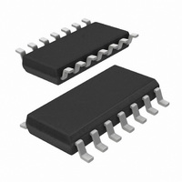
74LVC125AD,112 NXP Semiconductors, 74LVC125AD,112 Datasheet - Page 10

74LVC125AD,112
Manufacturer Part Number
74LVC125AD,112
Description
IC BUFF DVR TRI-ST QD 14SOICN
Manufacturer
NXP Semiconductors
Series
74LVCr
Datasheet
1.74LVC125ABQ115.pdf
(20 pages)
Specifications of 74LVC125AD,112
Logic Type
Buffer/Line Driver, Non-Inverting
Number Of Elements
4
Number Of Bits Per Element
1
Current - Output High, Low
24mA, 24mA
Voltage - Supply
2.7 V ~ 3.6 V
Operating Temperature
-40°C ~ 125°C
Mounting Type
Surface Mount
Package / Case
14-SOIC (3.9mm Width), 14-SOL
Logic Family
LVC
Number Of Channels Per Chip
4
Polarity
Non-Inverting
Supply Voltage (max)
3.6 V
Supply Voltage (min)
1.2 V
Maximum Operating Temperature
+ 125 C
Mounting Style
SMD/SMT
High Level Output Current
- 24 mA
Low Level Output Current
24 mA
Minimum Operating Temperature
- 40 C
Number Of Lines (input / Output)
4 / 4
Output Type
3-State
Propagation Delay Time
2.4 ns at 3.3 V
Lead Free Status / RoHS Status
Lead free / RoHS Compliant
Other names
74LVC125AD
74LVC125AD
935231700112
74LVC125AD
935231700112
Philips Semiconductors
2003 May 07
handbook, full pagewidth
Quad buffer/line driver with 5 V tolerant input/outputs;
3-state
Definitions for test circuit:
R
C
R
t
t
t
L
L
T
PLH
PLZ
PHZ
= Load resistor.
= Load capacitance including jig and probe capacitance.
= Termination resistance should be equal to the output impedance Z
/t
/t
/t
PZL
TEST
PHL
PZH
SWITCH POSITION
open
2
GND
SWITCH
V
CC
GENERATOR
PULSE
Fig.8 Load circuitry for switching times.
< 2.7 V
2.7 to 3.6 V
V I
V
CC
R T
D.U.T.
V CC
o
10
of the pulse generator.
V
2.7 V
CC
V O
V
I
50 pF
C L
500
500
R L
R L
S1
MNA368
2
open
GND
V CC
Product specification
74LVC125A


