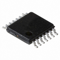
74LVT126PW,118 NXP Semiconductors, 74LVT126PW,118 Datasheet - Page 6

74LVT126PW,118
Manufacturer Part Number
74LVT126PW,118
Description
IC BUFF TRI-ST QD N-INV 14TSSOP
Manufacturer
NXP Semiconductors
Series
74LVTr
Datasheet
1.74LVT126D112.pdf
(15 pages)
Specifications of 74LVT126PW,118
Package / Case
14-TSSOP
Logic Type
Buffer/Line Driver, Non-Inverting
Number Of Elements
4
Number Of Bits Per Element
1
Current - Output High, Low
32mA, 64mA
Voltage - Supply
2.7 V ~ 3.6 V
Operating Temperature
-40°C ~ 85°C
Mounting Type
Surface Mount
Logic Family
LVT
Number Of Channels Per Chip
4
Polarity
Non-Inverting
Supply Voltage (max)
3.6 V
Supply Voltage (min)
2.7 V
Maximum Operating Temperature
+ 85 C
Mounting Style
SMD/SMT
High Level Output Current
- 32 mA
Input Bias Current (max)
7000 uA
Low Level Output Current
64 mA
Minimum Operating Temperature
- 40 C
Output Type
3-State
Propagation Delay Time
2.4 ns (Typ) @ 3.3 V
Number Of Lines (input / Output)
4 / 4
Lead Free Status / RoHS Status
Lead free / RoHS Compliant
Lead Free Status / RoHS Status
Lead free / RoHS Compliant, Lead free / RoHS Compliant
Other names
568-4628-2
74LVT126PW-T
74LVT126PW-T
935209470118
74LVT126PW-T
74LVT126PW-T
935209470118
Philips Semiconductors
Table 7:
At recommended operating conditions; voltages are referenced to GND (ground = 0 V).
[1]
[2]
[3]
[4]
[5]
[6]
11. Dynamic characteristics
Table 8:
GND = 0 V; t
9397 750 14553
Product data sheet
Symbol Parameter
I
I
I
I
C
C
Symbol Parameter
T
t
t
t
t
EX
PU
OZ
CC
PLH
PHL
PZH
PZL
I
amb
I
O
CC
, I
Typical values are measured at nominal V
Unused pins at V
This is the bus hold overdrive current required to force the input to the opposite logic state.
This parameter is valid for any V
a transition time of 100 s is permitted. This parameter is valid for T
Measured with outputs pulled up to V
This is the increase in supply current for each input at the specified voltage level other than V
PD
= 40 C to +85 C
external current into output output in HIGH-state when
power-up or power-down
3-state output current
3-state output current
quiescent supply current
additional supply current
per input pin
input capacitance
output capacitance
propagation delay nA to nY
propagation delay nA to nY
output enable time nOE to nY
output enable time nOE to nY
Static characteristics
Dynamic characteristics
r
= t
f
= 2.5 ns; C
CC
or GND.
[1]
L
= 50 pF; R
CC
…continued
between 0 V and 1.2 V with a transition time of up to 10 ms. From V
CC
Conditions
V
V
V
V
V
V
I
V
V
V
V
outputs disabled; V
O
or GND.
L
O
CC
CC
I
CC
CC
CC
CC
CC
I
output HIGH: V
output LOW: V
outputs HIGH
outputs LOW
outputs disabled
CC
= GND or V
= 0 A
= 0 V or V
= 500 ; for test circuit see
> V
= 3.0 V
= 3.6 V
= 3.6 V; V
= 3 V to 3.6 V; one input at
or GND
and T
1.2 V; V
0.6 V and other inputs at
CC
; V
Rev. 04 — 11 February 2005
amb
O
Conditions
V
V
V
V
V
V
V
V
CC
= 25 C.
= 5.5 V and
CC
CC
CC
CC
CC
CC
CC
CC
CC
O
I
= GND or V
= 0.5 V to V
; nOE = don’t care
O
= 2.7 V
= 3.3 V
= 2.7 V
= 3.3 V
= 2.7 V
= 3.3 V
= 2.7 V
= 3.3 V
O
= 0.5 V
O
= 3.0 V
= 0 V or 3.0 V
amb
0.3 V
0.3 V
0.3 V
0.3 V
CC
CC
= 25 C only.
;
;
Figure
7.
[4]
[5]
[6]
Min
-
-
-
-
-
-
-
-
-
-
CC
or GND.
Min
-
1.0
-
1.0
-
1.0
-
1.1
© Koninklijke Philips Electronics N.V. 2005. All rights reserved.
Typ
60
1
0.13
2
0.13
0.1
4
8
1
1
3.3 V quad buffer; 3-state
CC
= 1.2 V to V
Typ
-
2.3
-
2.4
-
3.6
-
3.6
74LVT126
Max
125
5
0.19
7
0.19
0.2
-
-
100
5
Max
4.5
3.8
4.4
3.9
6.1
5.4
5.8
5.2
CC
= 3.3 V
Unit
mA
mA
mA
mA
pF
pF
Unit
ns
ns
ns
ns
ns
ns
ns
ns
A
A
A
A
6 of 15
0.3 V


