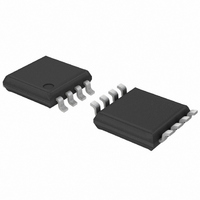
74LVC3G07DP,125 NXP Semiconductors, 74LVC3G07DP,125 Datasheet - Page 3

74LVC3G07DP,125
Manufacturer Part Number
74LVC3G07DP,125
Description
IC BUFFER TRPL OP/DRAIN 8TSSOP
Manufacturer
NXP Semiconductors
Series
74LVCr
Datasheet
1.74LVC3G07DC125.pdf
(21 pages)
Specifications of 74LVC3G07DP,125
Logic Type
Buffer/Line Driver, Non-Inverting with Open Drain
Number Of Elements
3
Number Of Bits Per Element
1
Current - Output High, Low
32mA, 32mA
Voltage - Supply
2 V ~ 5.5 V
Operating Temperature
-40°C ~ 125°C
Mounting Type
Surface Mount
Package / Case
8-TSSOP
Logic Family
LVC
Number Of Channels Per Chip
3
Polarity
Non-Inverting
Supply Voltage (max)
5.5 V
Supply Voltage (min)
1.65 V
Maximum Operating Temperature
+ 125 C
Mounting Style
SMD/SMT
Low Level Output Current
32 mA
Maximum Power Dissipation
250 mW
Minimum Operating Temperature
- 40 C
Number Of Lines (input / Output)
3 / 3
Output Type
Open Drain
Propagation Delay Time
3.7 ns
Lead Free Status / RoHS Status
Lead free / RoHS Compliant
Other names
74LVC3G07DP-G
74LVC3G07DP-G
935275558125
74LVC3G07DP-G
935275558125
NXP Semiconductors
5. Functional diagram
6. Pinning information
74LVC3G07
Product data sheet
Fig 1.
Fig 4.
Logic symbol
Pin configuration SOT505-2 and SOT765-1
1A
2A
3A
GND
1A
3Y
2A
6.1 Pinning
001aah762
1
2
3
4
1Y
2Y
3Y
74LVC3G07
001aab022
8
7
6
5
All information provided in this document is subject to legal disclaimers.
Fig 2.
V
1Y
3A
2Y
CC
Rev. 7 — 9 August 2010
IEC logic symbol
3A
1A
2A
001aah763
1
1
1
Fig 5.
1Y
3Y
2Y
Pin configuration SOT833-1, SOT1089,
SOT1116 and SOT1203
GND
Triple buffer with open-drain output
1A
3Y
2A
Fig 3.
Transparent top view
74LVC3G07
1
2
3
4
A
Logic diagram (one driver)
001aac022
74LVC3G07
8
7
6
5
V
1Y
3A
2Y
CC
© NXP B.V. 2010. All rights reserved.
GND
Y
mna591
3 of 21


