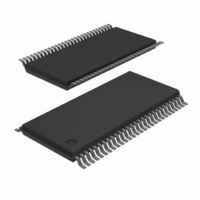
74LVT16646ADGG,118 NXP Semiconductors, 74LVT16646ADGG,118 Datasheet - Page 11

74LVT16646ADGG,118
Manufacturer Part Number
74LVT16646ADGG,118
Description
IC TRANSCVR 16BIT N-INV 56TSSOP
Manufacturer
NXP Semiconductors
Series
74LVTr
Datasheet
1.74LVT16646ADL512.pdf
(21 pages)
Specifications of 74LVT16646ADGG,118
Logic Type
Transceiver, Non-Inverting
Number Of Elements
2
Number Of Bits Per Element
8
Current - Output High, Low
32mA, 64mA
Voltage - Supply
2.7 V ~ 3.6 V
Operating Temperature
-40°C ~ 85°C
Mounting Type
Surface Mount
Package / Case
56-TSSOP
Lead Free Status / RoHS Status
Lead free / RoHS Compliant
Other names
74LVT16646ADG-T
74LVT16646ADG-T
935204690118
74LVT16646ADG-T
935204690118
Philips Semiconductors
Table 7:
At recommended operating conditions; voltages are referenced to GND (ground = 0 V).
[1]
[2]
[3]
[4]
[5]
[6]
[7]
11. Dynamic characteristics
Table 8:
GND = 0 V; t
9397 750 14326
Product data sheet
Symbol
C
C
Symbol
T
f
t
t
max
PLH
PHL
I
amb
I
I/O
CC
All typical values are measured at V
For valid test results, data must not be loaded into the flip-flops (or latches) after applying power.
Unused pins at V
This is the bus hold overdrive current required to force the input to the opposite logic state.
This parameter is valid for V
of 100 s is permitted. This parameter is valid for T
I
This is the increase in supply current for each input at the specified voltage level other than V
CC
= 40 C to +85 C
is measured with outputs pulled to V
Static characteristics
Dynamic characteristics
r
Parameter
additional supply
current per input pin
input capacitance
I/O pin capacitance
Parameter
maximum clock frequency V
propagation delay nAx to
nBx or nBx to nAx
propagation delay nCPAB
to nBx or nCPBA to nAx
propagation delay nSAB
to nBx or nSBA to nAx
propagation delay nAx to
nBx or nBx to nAx
propagation delay nCPAB
to nBx or nCPBA to nAx
propagation delay nSAB
to nBx or nSBA to nAx
= t
f
= 2.5 ns; C
CC
or GND.
[1]
L
CC
= 50 pF; R
= 0 V to 1.2 V with a transition time of up to 10 ms. From V
…continued
CC
Conditions
V
V
or GND
V
V
disabled
CC
CC
I
I/O
= 3.3 V and T
= 0 V or 3.0 V
CC
Conditions
Figure 6
see
see
see
see
see
see
L
= 0 V or 3.0 V; outputs
= 3 V to 3.6 V; one input at
CC
= 500 ; for input definitions see
or GND.
V
V
V
V
V
V
V
V
V
V
V
V
0.6 V, other inputs at V
CC
CC
CC
CC
CC
CC
CC
CC
CC
CC
CC
CC
Figure 8
Figure 6
Figure 7
Figure 8
Figure 6
Figure 7
= 3.3 V
= 3.3 V
= 2.7 V
= 3.3 V
= 2.7 V
= 3.3 V
= 2.7 V
= 3.3 V
= 2.7 V
= 3.3 V
= 2.7 V
= 3.3 V
= 2.7 V
Rev. 03 — 12 January 2005
amb
amb
= 25 C only.
= 25 C.
0.3 V; see
0.3 V
0.3 V
0.3 V
0.3 V
0.3 V
0.3 V
CC
[7]
Figure
Min
-
-
-
Min
150
0.5
-
1.5
-
1.0
-
0.5
-
1.5
-
1.0
-
3.3 V 16-bit bus transceiver; 3-state
13; for test circuit see
CC
= 1.2 V to 3.3 V
CC
Typ
0.1
3
9
or GND.
Typ
-
1.9
-
2.7
-
2.5
-
1.9
-
2.4
-
2.8
-
© Koninklijke Philips Electronics N.V. 2005. All rights reserved.
74LVT16646A
Max
0.2
-
-
Max
-
3.7
4.3
4.5
5.3
4.6
5.4
3.7
4.4
4.5
5.2
4.8
5.6
0.3 V. A transition time
Figure
14.
Unit
mA
pF
pF
Unit
MHz
ns
ns
ns
ns
ns
ns
ns
ns
ns
ns
ns
ns
11 of 21


