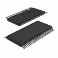
74ABT16827ADGG,118 NXP Semiconductors, 74ABT16827ADGG,118 Datasheet - Page 4

74ABT16827ADGG,118
Manufacturer Part Number
74ABT16827ADGG,118
Description
IC BUFF DVR TRI-ST 20BIT 56TSSOP
Manufacturer
NXP Semiconductors
Series
74ABTr
Datasheet
1.74ABT16827ADGG118.pdf
(10 pages)
Specifications of 74ABT16827ADGG,118
Logic Type
Buffer/Line Driver, Non-Inverting
Number Of Elements
2
Number Of Bits Per Element
10
Current - Output High, Low
32mA, 64mA
Voltage - Supply
4.5 V ~ 5.5 V
Operating Temperature
-40°C ~ 85°C
Mounting Type
Surface Mount
Package / Case
56-TSSOP
Logic Family
ABT
Number Of Channels Per Chip
20
Polarity
Non-Inverting
Supply Voltage (max)
5.5 V
Supply Voltage (min)
4.5 V
Maximum Operating Temperature
+ 85 C
Mounting Style
SMD/SMT
High Level Output Current
- 32 mA
Low Level Output Current
64 mA
Minimum Operating Temperature
- 40 C
Output Type
3-State
Propagation Delay Time
2.4 ns at 5 V
Lead Free Status / RoHS Status
Lead free / RoHS Compliant
Other names
74ABT16827ADG-T
74ABT16827ADG-T
935203520118
74ABT16827ADG-T
935203520118
Philips Semiconductors
LOGIC DIAGRAM
ABSOLUTE MAXIMUM RATINGS
NOTES:
1. Stresses beyond those listed may cause permanent damage to the device. These are stress ratings only and functional operation of the
2. The performance capability of a high-performance integrated circuit in conjunction with its thermal environment can create junction
3. The input and output voltage ratings may be exceeded if the input and output current ratings are observed.
RECOMMENDED OPERATING CONDITIONS
2002 Dec 17
SYMBOL
SYMBOL
SYMBOL
20-bit buffer/line driver, non-inverting (3-State)
nOE1
nOE2
device at these or any other conditions beyond those indicated under “recommended operating conditions” is not implied. Exposure to
absolute-maximum-rated conditions for extended periods may affect device reliability.
temperatures which are detrimental to reliability. The maximum junction temperature of this integrated circuit should not exceed 150 C.
V
T
I
I
V
V
T
I
O
OUT
V
I
V
I
amb
I
OK
OUT
OH
t/ v
V
V
OL
stg
CC
IK
CC
IH
IL
I
I
DC supply voltage
DC input diode current
DC input voltage
DC output diode current
DC output voltage
DC output current
DC output current
Storage temperature range
DC supply voltage
Input voltage
HIGH-level input voltage
LOW-level Input voltage
HIGH-level output current
LOW-level output current
Input transition rise or fall rate
Operating free-air temperature range
nY0
nA0
PARAMETER
3
3
nY1
nA1
1, 2
PARAMETER
PARAMETER
nY2
nA2
nY3
nA3
Output in Off or HIGH state
4
Output in HIGH state
Output in LOW state
nY4
nA4
CONDITIONS
V
V
O
I
< 0 V
< 0 V
nA5
nY5
nA6
nY6
MIN
–40
4.5
2.0
0
–
–
–
0
LIMITS
–0.5 to +7.0
–1.2 to +7.0
–0.5 to +5.5
–65 to 150
nY7
nA7
RATING
74ABTH16827A
–18
–50
128
–64
74ABT16827A
MAX
V
–32
+85
5.5
0.8
64
10
–
CC
nY8
nA8
Product data
SH00013
UNIT
UNIT
UNIT
ns/V
mA
mA
mA
mA
mA
mA
V
V
V
V
V
V
V
C
C
nA9
nY9


