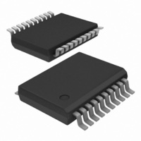
74LVT640DB,118 NXP Semiconductors, 74LVT640DB,118 Datasheet - Page 2

74LVT640DB,118
Manufacturer Part Number
74LVT640DB,118
Description
IC TRANSCEIVER 8BIT INV 20SSOP
Manufacturer
NXP Semiconductors
Series
74LVTr
Datasheet
1.74LVT640DB112.pdf
(10 pages)
Specifications of 74LVT640DB,118
Logic Type
Transceiver, Inverting
Number Of Elements
1
Number Of Bits Per Element
8
Current - Output High, Low
32mA, 64mA
Voltage - Supply
2.7 V ~ 3.6 V
Operating Temperature
-40°C ~ 85°C
Mounting Type
Surface Mount
Package / Case
20-SSOP
Lead Free Status / RoHS Status
Lead free / RoHS Compliant
Other names
74LVT640DB-T
74LVT640DB-T
935213080118
74LVT640DB-T
935213080118
Philips Semiconductors
FEATURES
QUICK REFERENCE DATA
ORDERING INFORMATION
PIN CONFIGURATION
20-Pin Plastic SO
20-Pin Plastic SSOP
20-Pin Plastic TSSOP
1998 Feb 19
Octal bidirectional bus interface
3-State buffers
Output capability: +64mA/-32mA
TTL input and output switching levels
Input and output interface capability to systems at 5V supply
Bus-hold data inputs eliminate the need for external pull-up
resistors to hold unused inputs
Live insertion/extraction permitted
Power-up 3-State
No bus current loading when output is tied to 5V bus
Latch-up protection exceeds 500mA per JEDEC Std 17
ESD protection exceeds 2000V per MIL STD 883 Method 3015
and 200V per Machine Model
3.3V Octal transceiver with direction pin; inverting
(3-State)
SYMBOL
I
t
t
C
C
PLH
PHL
CCZ
I/O
IN
PACKAGES
GND
DIR
A0
A1
A2
A3
A4
A5
A6
A7
Propagation delay
An to Bn or Bn to An
Input capacitance
DIR, OE
I/O pin capacitance
Total supply current
10
1
2
3
4
5
6
7
8
9
SV00014
PARAMETER
TEMPERATURE RANGE
20
19
18
17
16
15
14
13
12
11
V
OE
B0
B1
B2
B3
B4
B5
B6
B7
–40 C to +85 C
–40 C to +85 C
–40 C to +85 C
CC
C
V
V
Outputs disabled; V
Outputs disabled; V
CC
I
L
= 0V or 3.0V
OUTSIDE NORTH AMERICA
= 50pF;
= 3.3V
2
T
amb
DESCRIPTION
The LVT640 is a high-performance BiCMOS product designed for
V
This device is an octal transceiver featuring inverting 3-State bus
compatible outputs in both send and receive directions. The control
function implementation minimizes external timing requirements.
The device features an Output Enable (OE) input for easy cascading
and a Direction (DIR) input for direction control.
PIN DESCRIPTION
74LVT640 PW
74LVT640 DB
74LVT640 D
CC
2, 3, 4, 5, 6, 7, 8, 9
18, 17, 16, 15, 14,
CONDITIONS
PIN NUMBER
= 25 C; GND = 0V
operation at 3.3V.
13, 12, 11
I/O
19
10
20
CC
1
= 0V or 3.0V
= 3.6V
SYMBOL
A0 – A7
B0 – B7
NORTH AMERICA
74LVT640PW DH
GND
V
DIR
OE
74LVT640 DB
CC
74LVT640 D
Direction control input
Data inputs/outputs (A side)
Data inputs/outputs (B side)
Output enable input
(active–Low)
Ground (0V)
Positive supply voltage
TYPICAL
NAME AND FUNCTION
0.13
2.3
2.4
4
7
Product specification
74LVT640
PKG. DWG. #
853-1881 18988
SOT163-1
SOT339-1
SOT360-1
UNIT
mA
ns
pF
pF


