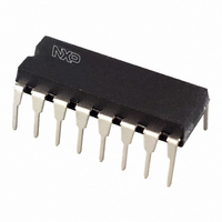
74HCT7403N,112 NXP Semiconductors, 74HCT7403N,112 Datasheet - Page 17

74HCT7403N,112
Manufacturer Part Number
74HCT7403N,112
Description
IC FIFO REGISTER 64X4 3ST 16DIP
Manufacturer
NXP Semiconductors
Series
74HCTr
Datasheets
1.74HCT4046ADB112.pdf
(19 pages)
2.74HCT4046ADB112.pdf
(23 pages)
3.74HCT7403N112.pdf
(28 pages)
Specifications of 74HCT7403N,112
Function
Asynchronous, Synchronous
Memory Size
256 (64 x 4)
Data Rate
15MHz
Voltage - Supply
4.5 V ~ 5.5 V
Mounting Type
Through Hole
Package / Case
16-DIP (0.300", 7.62mm)
Lead Free Status / RoHS Status
Lead free / RoHS Compliant
Operating Temperature
-
Access Time
-
Other names
568-2904-5
933999380112
933999380112
Philips Semiconductors
DEFINITIONS OF SYMBOLS AND TERMS USED IN
HCMOS DATA SHEETS
Currents
Positive current is defined as conventional current flow
into a device.
Negative current is defined as conventional current flow
out of a device.
Voltages
All voltages are referenced to GND (ground), which is
typically 0 V.
March 1988
I
I
I
I
I
I
I
I
GND
V
V
V
V
CC
GND
I
IK
O
OK
OZ
S
I
CC
EE
H
IH
HCMOS family characteristics
CC
Quiescent power supply current; the current
flowing into the V
Additional quiescent supply current per input
pin at a specified input voltage and V
Quiescent power supply current; the current
flowing into the GND terminal.
Input leakage current; the current flowing into a
device at a specified input voltage and V
Input diode current; the current flowing into a
device at a specified input voltage.
Output source or sink current: the current
flowing into a device at a specified output
voltage.
Output diode current; the current flowing into a
device at a specified output voltage.
OFF-state output current; the leakage current
flowing into the output of a 3-state device in the
OFF-state, when the output is connected to
V
Analog switch leakage current; the current
flowing into an analog switch at a specified
voltage across the switch and V
Supply voltage; for a device with a single
negative power supply, the most negative
power supply, used as the reference level for
other voltages; typically ground.
Supply voltage; the most positive potential on
the device.
Supply voltage; one of two (GND and V
negative power supplies.
Hysteresis voltage; difference between the
trigger levels, when applying a positive and a
negative-going input signal.
HIGH level input voltage; the range of input
voltages that represents a logic HIGH level in
the system.
CC
or GND.
CC
supply terminal.
CC
.
CC
.
EE
CC
)
.
17
Analog terms
Capacitances
V
V
V
V
V
R
C
C
C
C
C
IL
OH
OL
T
T
R
ON
I
I/O
L
PD
S
ON
LOW level input voltage; the range of input
voltages that represents a logic LOW level in
the system.
HIGH level output voltage; the range of
voltages at an output terminal with a specified
output loading and supply voltage. Device
inputs are conditioned to establish a HIGH level
at the output.
LOW level output voltage; the range of voltages
at an output terminal with a specified output
loading and supply voltage. Device inputs are
conditioned to establish a LOW level at the
output.
Trigger threshold voltage; positive-going signal.
Trigger threshold voltage; negative-going
signal.
ON-resistance; the effective ON-state
resistance of an analog switch, at a specified
voltage across the switch and output load.
ON-resistance between any two switches of an
analog device at a specified voltage across the
switch and output load.
Input capacitance; the capacitance measured
at a terminal connected to an input of a device.
Input/Output capacitance; the capacitance
measured at a terminal connected to an I/O-pin
(e.g. a transceiver).
Output load capacitance; the capacitance
connected to an output terminal including jig
and probe capacitance.
Power dissipation capacitance; the capacitance
used to determine the dynamic power
dissipation per logic function, when no extra
load is provided to the device.
Switch capacitance; the capacitance of a
terminal to a switch of an analog device.
ON-resistance; the difference in
FAMILY SPECIFICATIONS


