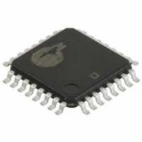
CY7C4241V-15AXC Cypress Semiconductor Corp, CY7C4241V-15AXC Datasheet - Page 6

CY7C4241V-15AXC
Manufacturer Part Number
CY7C4241V-15AXC
Description
IC SYNC FIFO MEM 4KX9 32-TQFP
Manufacturer
Cypress Semiconductor Corp
Series
CY7Cr
Specifications of CY7C4241V-15AXC
Function
Synchronous
Memory Size
36K (4K x 9)
Data Rate
100MHz
Access Time
10ns
Voltage - Supply
3.3V
Operating Temperature
-40°C ~ 85°C
Mounting Type
Surface Mount
Package / Case
32-TQFP
Configuration
Dual
Density
36Kb
Access Time (max)
11ns
Word Size
9b
Organization
4Kx9
Sync/async
Synchronous
Expandable
Yes
Bus Direction
Uni-Directional
Package Type
TQFP
Clock Freq (max)
66.7MHz
Operating Supply Voltage (typ)
3.3V
Operating Supply Voltage (min)
3V
Operating Supply Voltage (max)
3.6V
Supply Current
20mA
Operating Temp Range
0C to 70C
Operating Temperature Classification
Commercial
Mounting
Surface Mount
Pin Count
32
Lead Free Status / RoHS Status
Lead free / RoHS Compliant
Available stocks
Company
Part Number
Manufacturer
Quantity
Price
Company:
Part Number:
CY7C4241V-15AXC
Manufacturer:
CY
Quantity:
21
Company:
Part Number:
CY7C4241V-15AXC
Manufacturer:
Cypress Semiconductor Corp
Quantity:
10 000
Company:
Part Number:
CY7C4241V-15AXCT
Manufacturer:
Cypress Semiconductor Corp
Quantity:
10 000
Programmable Flag (PAE, PAF) Operation
Whether the flag offset registers are programmed as described
in
Almost Empty Flag (PAE) and programmable Almost Full Flag
(PAF) states are determined by their corresponding offset
registers and the difference between the read and write pointers.
Table 1. Writing the Offset Registers
The number formed by the empty offset least significant bit
register and empty offset most significant register is referred to
as n and determines the operation of PAE. PAE is synchronized
to the LOW-to-HIGH transition of RCLK by one flip-flop and is
Table 2. Status Flags
Document #: 38-06010 Rev. *C
Notes
0
1 to n
(n+1) to 32
33 to (64−(m+1))
(64−m)
64
0
1 to n
(n+1) to 512
513 to (1024 −(m+1))
(1024−m)
1024
LD
1. The same selection sequence applies to reading from the registers. REN1 and REN2 are enabled and a read is performed on the LOW-to-HIGH transition of RCLK.
2. n = Empty Offset (n=7 default value).
3. m = Full Offset (m=7 default value).
0
0
1
1
Table 1
CY7C4221V
[2]
[2]
WEN
[3]
0
1
0
1
CY7C4421V
to 63
[3]
or the default values are used, the programmable
to 1023
WCLK
[1]
0
1 to n
(n+1) to 1024
1025 to (2048 −(m+1))
(2048−m)
2048
Empty Offset (LSB)
Empty Offset (MSB)
Full Offset (LSB)
Full Offset (MSB)
No Operation
Write Into FIFO
No Operation
[2]
CY7C4231V
0
1 to n
(n+1) to 128
129 to (256−(m+1))
(256−m)
256
[3]
Number of Words in FIFO
Number of Words in FIFO
to 2047
[2]
Selection
[3]
CY7C4201V
to 255
0
1 to n
(n+1) to 2048
2049 to (4096 −(m+1))
(4096−m)
4096
[2]
CY7C4241V
[3]
to 4095
0
1 to n
(n+1) to 256
257 to (512−(m+1))
(512−m)
512
LOW when the FIFO contains n or fewer unread words. PAE is
set HIGH by the LOW-to-HIGH transition of RCLK when the
FIFO contains (n+1) or greater unread words.
The number formed by the full offset least significant bit register
and full offset most significant bit register is referred to as m and
determines the operation of PAF.
LOW-to-HIGH transition of WCLK by one flip-flop and is set LOW
when the number of unread words in the FIFO is greater than or
equal to CY7C4421V (64 – m), CY7C4201V (256 – m),
CY7C4211V (512 – m), CY7C4221V (1K – m), CY7C4231V (2K
– m), CY7C4241V (4K – m), and CY7C4251V (8K – m). PAF is
set HIGH by the LOW-to-HIGH transition of WCLK when the
number of available memory locations is greater than m.
[2]
[3]
CY7C4211V
(n+1) to 4096
0
1 to n
4097 to (8192 −(m+1))
(8192−m)
8192
to 511
[2]
CY7C4251V
[3]
to 8191
CY7C4201V/4211V/4221V
FF
H
H
H
H
H
L
CY7C4241V/4251V
FF
H
H
H
H
H
L
PAE is synchronized to the
PAF
H
H
H
H
L
L
PAF
H
H
H
H
L
L
PAE
PAE
H
H
H
H
L
L
H
H
H
H
L
L
Page 6 of 19
EF
EF
H
H
H
H
H
H
H
H
H
H
L
L
[+] Feedback


