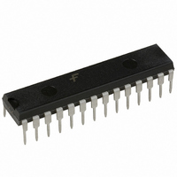
74ACT2708PC Fairchild Semiconductor, 74ACT2708PC Datasheet

74ACT2708PC
Specifications of 74ACT2708PC
Available stocks
Related parts for 74ACT2708PC
74ACT2708PC Summary of contents
Page 1
... Ordering Code: Order Number Package Number 74ACT2708PC N28B 28-Lead Plastic Dual-In-Line Package (PDIP), JEDEC MS-010, 0.600” Wide Device also available in Tape and Reel. Specify by appending suffix letter “X” to the ordering code. Connection Diagram ...
Page 2
Logic Symbol Block Diagram www.fairchildsemi.com 2 ...
Page 3
Functional Description INPUTS Data Inputs (D – Data inputs for 9-bit wide data are TTL-compatible. Word width can be reduced by trying unused inputs to ground and leaving the corresponding outputs open. Reset (MR) Reset is accomplished ...
Page 4
MODES OF OPERATION Mode 1: Shift in Sequence for FIFO Empty to Full Sequence of Operation 1. Input Ready is initially HIGH; HF and FULL flags are LOW. The FIFO is empty and prepared for valid data LOW ...
Page 5
Mode 2: Master Reset Sequence of Operation 1. Input and Output Ready, HF and FULL can be in any state before the reset sequence with Master Reset (MR) HIGH. 2. Master Reset goes LOW and clears the FIFO, setting up ...
Page 6
Mode 3: With FIFO Full, Shift-In is Held HIGH in Anticipation of an Empty Location Sequence of Operation 1. The FIFO is initially full and Shift-In goes HIGH initially HIGH. Shift-Out is LOW LOW. 2. Shift-Out ...
Page 7
Mode 4: Shift-Out Sequence, FIFO Full to Empty Sequence of Operation 1. FIFO is initially full and OR is HIGH, indicating valid data is at the output LOW goes HIGH, resulting in OR going LOW one ...
Page 8
Mode 5: With FIFO Empty, Shift-Out is Held HIGH in Anticipation of Data Sequence of Operation 1. FIFO is initially empty; Shift-Out goes HIGH. 2. Shift-In pulse loads data into the FIFO and IR falls. HF rises propagation delay t ...
Page 9
FIFO Expansion Word Width Expansion Word width can be increased by connecting the corresponding input control signals of multiple devices. Flags can be mon- itored to obtain a composite signal by ANDing the corresponding flags. Note: AND the corresponding flags ...
Page 10
Absolute Maximum Ratings Supply Voltage ( Input Diode Current ( 0. 0. Input Voltage ( Output Diode Current ( ...
Page 11
AC Electrical Characteristics Symbol Parameter t Propagation Delay, t PLH Propagation Delay, t PHL Propagation Delay, t PLH IHF Propagation Delay, t PHL ...
Page 12
AC Electrical Characteristics Symbol Parameter t HF Pulse Width Pulse Width Pulse Width Fall-Through Times, t PLH Output Enable PZL OE ...
Page 13
Physical Dimensions inches (millimeters) unless otherwise noted 28-Lead Plastic Dual-In-Line Package (PDIP), JEDEC MS-010, 0.600” Wide LIFE SUPPORT POLICY FAIRCHILD’S PRODUCTS ARE NOT AUTHORIZED FOR USE AS CRITICAL COMPONENTS IN LIFE SUPPORT DEVICES OR SYSTEMS WITHOUT THE EXPRESS WRITTEN APPROVAL ...


