74AC175SC Fairchild Semiconductor, 74AC175SC Datasheet
74AC175SC
Specifications of 74AC175SC
Available stocks


Related parts for 74AC175SC


74AC175SC Summary of contents
Page 1
... I Asynchronous common reset I True and complement output I Outputs source/sink 24mA I ACT175 has TTL-compatible inputs I Ordering Information Order Package Number Number 74AC175SC M16A 74AC175SJ M16D 74AC175MTC MTC16 74AC175PC N16E 74ACT175SC M16A 74ACT175SJ M16D 74ACT175MTC MTC16 Device also available in Tape and Reel. Specify by appending suffix letter “X” to the ordering number. ...
Page 2
... IEEE/IEC Logic Diagram Please note that this diagram is provided only for the understanding of logic operations and should not be used to estimate propagation delays. ©1988 Fairchild Semiconductor Corporation 74AC175, 74ACT175 Rev. 1.4 Functional Description The AC/ACT175 consists of four edge-triggered D-type flip-flops with individual D inputs and Q and Q outputs. ...
Page 3
... O T Operating Temperature A ∆V / ∆t Minimum Input Edge Rate, AC Devices: V from 30 ∆V / ∆t Minimum Input Edge Rate, ACT Devices: V from 0.8V to 2.0V ©1988 Fairchild Semiconductor Corporation 74AC175, 74ACT175 Rev. 1.4 Parameter Parameter , V @ 3.3V, 4.5V, 5. 4.5V, 5. Rating –0.5V to +7.0V –20mA +20mA – ...
Page 4
... Notes: 1. All outputs loaded; thresholds on input associated with output under test. 2. Maximum test duration 2.0ms, one output loaded at a time and I @ 3.0V are guaranteed to be less than or equal to the respective limit @ 5. ©1988 Fairchild Semiconductor Corporation 74AC175, 74ACT175 Rev. 1 +25° (V) Conditions Typ ...
Page 5
... Minimum Dynamic OLD (5) Output Current I OHD I Maximum Quiescent CC Supply Current Notes: 4. All outputs loaded; thresholds on input associated with output under test. 5. Maximum test duration 2.0ms, one output loaded at a time. ©1988 Fairchild Semiconductor Corporation 74AC175, 74ACT175 Rev. 1 +25° (V) Conditions Typ ...
Page 6
... Pulse Width, W HIGH or LOW t MR Pulse Width, LOW W t Recovery Time REC Note: 7. Voltage range 3.3 is 3.3V ± 0.3V. Voltage range 5.0 is 5.0V ± 0.5V. ©1988 Fairchild Semiconductor Corporation 74AC175, 74ACT175 Rev. 1 +25° 50pF L (6) V (V) Min. Typ. Max. CC 3.3 ...
Page 7
... MR Pulse Width, LOW W t Recovery Time rec Note: 9. Voltage Range 5.0 is 5.0V ± 0.5V. Capacitance Symbol Parameter C Input Capacitance IN C Power Dissipation Capacitance PD ©1988 Fairchild Semiconductor Corporation 74AC175, 74ACT175 Rev. 1 +25° 50pF L (8) V (V) Min. Typ. Max. CC 5.0 175 236 5 ...
Page 8
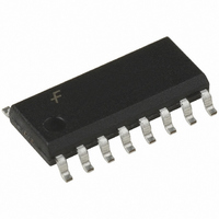
... Physical Dimensions Dimensions are in millimeters unless otherwise noted. Figure 2. 16-Lead Small Outline Integrated Circuit (SOIC), JEDEC MS-012, 0.150" Narrow ©1988 Fairchild Semiconductor Corporation 74AC175, 74ACT175 Rev. 1.4 Package Number M16A 8 www.fairchildsemi.com ...
Page 9
... Physical Dimensions (Continued) Dimensions are in millimeters unless otherwise noted. Figure 3. 16-Lead Small Outline Package (SOP), EIAJ TYPE II, 5.3mm Wide ©1988 Fairchild Semiconductor Corporation 74AC175, 74ACT175 Rev. 1.4 Package Number M16D 9 www.fairchildsemi.com ...
Page 10
... Physical Dimensions (Continued) Dimensions are in millimeters unless otherwise noted. 5.00±0.10 4.55 0.11 MTC16rev4 Figure 4. 16-Lead Thin Shrink Small Outline Package (TSSOP), JEDEC MO-153, 4.4mm Wide ©1988 Fairchild Semiconductor Corporation 74AC175, 74ACT175 Rev. 1.4 0.65 4.4±0.1 1.45 Package Number MTC16 10 5.90 4 ...
Page 11
... Physical Dimensions (Continued) Dimensions are in inches (millimeters) unless otherwise noted. Figure 5. 16-Lead Plastic Dual-In-Line Package (PDIP), JEDEC MS-001, 0.300” Wide ©1988 Fairchild Semiconductor Corporation 74AC175, 74ACT175 Rev. 1.4 Package Number N16E 11 www.fairchildsemi.com ...
Page 12
... TRADEMARKS The following are registered and unregistered trademarks Fairchild Semiconductor owns or is authorized to use and is not intended exhaustive list of all such trademarks. ® ACEx Across the board. Around the world.¥ ActiveArray¥ Bottomless¥ Build it Now¥ CoolFET¥ CROSSVOLT¥ ...