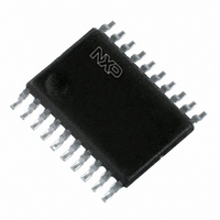
74LVT574PW,118 NXP Semiconductors, 74LVT574PW,118 Datasheet - Page 8

74LVT574PW,118
Manufacturer Part Number
74LVT574PW,118
Description
IC OCTAL D TRANSP F-F 20TSSOP
Manufacturer
NXP Semiconductors
Series
74LVTr
Type
D-Type Busr
Datasheet
1.74LVT574PW118.pdf
(16 pages)
Specifications of 74LVT574PW,118
Package / Case
20-TSSOP
Function
Standard
Output Type
Tri-State Non Inverted
Number Of Elements
1
Number Of Bits Per Element
8
Frequency - Clock
150MHz
Delay Time - Propagation
3.6ns
Trigger Type
Positive Edge
Current - Output High, Low
32mA, 64mA
Voltage - Supply
2.7 V ~ 3.6 V
Operating Temperature
-40°C ~ 85°C
Mounting Type
Surface Mount
Number Of Circuits
1
Logic Family
LVT
Logic Type
D-Type Edge Triggered Flip-Flop
Polarity
Non-Inverting
Input Type
Single-Ended
Propagation Delay Time
4.3 ns at 3.3 V
High Level Output Current
- 32 mA
Supply Voltage (max)
3.6 V
Maximum Operating Temperature
+ 85 C
Mounting Style
SMD/SMT
Minimum Operating Temperature
- 40 C
Supply Voltage (min)
2.7 V
Lead Free Status / RoHS Status
Lead free / RoHS Compliant
Lead Free Status / RoHS Status
Lead free / RoHS Compliant, Lead free / RoHS Compliant
Other names
568-4634-2
74LVT574PW-T
74LVT574PW-T
935176370118
74LVT574PW-T
74LVT574PW-T
935176370118
Available stocks
Company
Part Number
Manufacturer
Quantity
Price
NXP Semiconductors
11. Waveforms
74LVT_LVTH574_4
Product data sheet
Fig 6.
Fig 7.
Fig 9.
Qn output
OE input
GND
GND
Measurement points are given in
V
Propagation delay clock input (CP) to output (Qn), pulse width clock (CP) and maximum clock frequency
Measurement points are given in
V
with the output load.
Output enable time to HIGH-state and output
disable time from HIGH-state
Measurement points are given in
Remark: The shaded areas indicate when the input is permitted to change for predictable output performance.
Data setup and hold times
V
OL
OH
OL
V
I
and V
and V
OH
OH
are typical voltage output levels that occur with the output load.
are typical voltage output levels that occur
V
M
t
PZH
CP input
Dn input
Qn output
CP input
V
M
GND
GND
GND
V
V
V
V
l
l
OH
OL
V
Table 8
Table 8
Table 8
V
I
M
t
PHZ
001aae468
Rev. 04 — 11 September 2008
t
V
V
su(H)
M
Y
V
M
t
PHL
t
WH
V
t
h(H)
M
V
M
1/f
V
M
max
Fig 8.
t
WL
Qn output
OE input
74LVT574; 74LVTH574
3.0 V
GND
Measurement points are given in
V
with the output load.
Output enable time to LOW-state and output
disable time from LOW-state
V
OL
OL
V
I
and V
V
t
t
su(L)
M
PLH
OH
3.3 V octal D-type flip-flop; 3-state
are typical voltage output levels that occur
t
V
001aac445
V
h(L)
V
M
M
t
M
PZL
001aac738
V
M
Table 8
V
M
© NXP B.V. 2008. All rights reserved.
t
PLZ
001aae469
V
X
8 of 16


