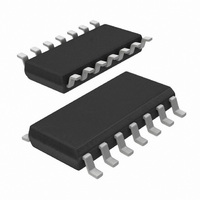
HEF4013BT,653 NXP Semiconductors, HEF4013BT,653 Datasheet - Page 13

HEF4013BT,653
Manufacturer Part Number
HEF4013BT,653
Description
IC FLIP FLOP DUAL DTYPE 14SOIC
Manufacturer
NXP Semiconductors
Series
4000Br
Type
D-Typer
Specifications of HEF4013BT,653
Package / Case
14-SOIC (3.9mm Width), 14-SOL
Function
Set(Preset) and Reset
Output Type
Differential
Number Of Elements
2
Number Of Bits Per Element
1
Frequency - Clock
40MHz
Trigger Type
Positive Edge
Current - Output High, Low
3.4mA, 3.4mA
Voltage - Supply
3 V ~ 15 V
Operating Temperature
-40°C ~ 125°C
Mounting Type
Surface Mount
Number Of Circuits
2
Logic Family
HEF4000
Logic Type
D-Type Edge Triggered Flip-Flop
Polarity
Inverting/Non-Inverting
Input Type
Single-Ended
Propagation Delay Time
30 ns at 15 V
High Level Output Current
- 4.2 mA
Low Level Output Current
4.2 mA
Supply Voltage (max)
15.5 V
Maximum Operating Temperature
+ 125 C
Mounting Style
SMD/SMT
Minimum Operating Temperature
- 40 C
Supply Voltage (min)
4.5 V
Lead Free Status / RoHS Status
Lead free / RoHS Compliant
Delay Time - Propagation
-
Lead Free Status / Rohs Status
Lead free / RoHS Compliant
Other names
933372660653
HEF4013BTD-T
HEF4013BTD-T
HEF4013BTD-T
HEF4013BTD-T
Available stocks
Company
Part Number
Manufacturer
Quantity
Price
Part Number:
HEF4013BT,653
Manufacturer:
NEXPERIA/安世
Quantity:
20 000
Philips Semiconductors
AC switching parameters
January 1995
f
f
f
t
t
t
t
t
t
t
i
o
max
r
PLH
PHL
TLH
THL
W
hold
, t
f
Input frequency; for combinatorial logic devices
the maximum number of inputs and outputs
switching in accordance with the device truth
table. For sequential logic devices the clock
frequency using alternate HIGH and LOW for
data input or using the toggle mode, whichever is
applicable.
Output frequency; each output.
Clock frequency; clock input waveform should
have a 50% duty cycle and be such as to cause
the outputs to be switching from 10%V
90%V
table.
Clock input rise and fall times; 10% and 90%
value.
Propagation delay time; the time between the
specified reference points, normally the 50%
points on the input and output waveforms, with
the output changing from the defined LOW level
to the defined HIGH level.
Propagation delay time; the time between the
specified reference points, normally the 50%
points on the input and output waveforms, with
the output changing from the defined HIGH level
to the defined LOW level.
Transition time, LOW-to-HIGH; the time between
two specified reference points on a waveform,
normally 10% and 90% points, that is changing
from LOW to HIGH.
Transition time, HIGH-to-LOW; the time between
two specified reference points on a waveform,
normally 90% and 10% points, that is changing
from HIGH to LOW.
Pulse width; the time between the 50% amplitude
points on the leading and trailing edges of a
pulse.
Hold time; the interval immediately following the
active transition of the timing pulse (usually the
clock pulse) or following the transition of the
control input to its latching level, during which
interval the data to be recognized must be
maintained at the input to ensure their continued
recognition. A negative hold time indicates that
the correct logic level may be released prior to
the timing pulse and still be recognized.
DD
in accordance with the device truth
DD
to
13
t
t
t
t
t
t
su
PHZ
PLZ
PZH
PZL
R
Set-up time; the interval immediately preceding
the active transition of the timing pulse (usually
the clock pulse) or preceding the transition of the
control input to its latching level, during which
interval the data to be recognized must be
maintained at the input to ensure their
recognition. A negative set-up time indicates that
the correct logic level may be initiated sometime
after the active transition of the timing pulse and
still be recognized.
3-state output disable time, HIGH to Z; the time
between the specified reference points, normally
the 50% point on the output enable input voltage
waveform and a point representing a 0.1 V
drop on the output voltage waveform of a 3-state
device, with the output changing from the output
HIGH level (V
3-state output disable time, LOW to Z; the time
between the specified reference points, normally
the 50% point on the output enable input voltage
waveform and a point representing a
0.1 (V
waveform of a 3-state device, with the output
changing from the output LOW level (V
high impedance OFF-state.
3-state output enable time, Z to HIGH; the time
between the specified reference points, normally
the 50% point on the output enable input voltage
waveform and a point representing a 0.1 V
on the output voltage waveform of a 3-state
device, with the output changing from a high
impedance OFF-state to the output HIGH level
(V
3-state output enable time, Z to LOW; the time
between the specified reference points, normally
the 50% point on the output enable input voltage
waveform and a point representing a
0.1 (V
voltage waveform of a 3-state device, with the
output changing from a high impedance
OFF-state to the output LOW level (V
Recovery time; the time between the end of an
overriding asynchronous input, typically a clear or
reset input, and the earliest permissible
beginning of a synchronous control input,
typically a clock input, normally measured at 50%
points on both input voltage waveforms.
OH
).
DD
DD
V
V
OL
OL
OH
) rise on the output voltage
) voltage drop on the output
Family Specifications
) to a high impedance OFF-state.
OL
OL
).
) to a
OH
OH
rise


