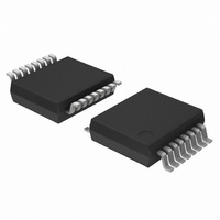
74HCT109DB,112 NXP Semiconductors, 74HCT109DB,112 Datasheet - Page 12

74HCT109DB,112
Manufacturer Part Number
74HCT109DB,112
Description
IC DUAL JK F-F POS-EDGE 16-SSOP
Manufacturer
NXP Semiconductors
Series
74HCTr
Type
JK Typer
Datasheets
1.74HCT4046ADB112.pdf
(19 pages)
2.74HCT4046ADB112.pdf
(23 pages)
3.74HC109D652.pdf
(9 pages)
Specifications of 74HCT109DB,112
Output Type
Differential
Package / Case
16-SSOP
Function
Set(Preset) and Reset
Number Of Elements
2
Number Of Bits Per Element
1
Frequency - Clock
55MHz
Delay Time - Propagation
13ns
Trigger Type
Positive Edge
Voltage - Supply
4.5 V ~ 5.5 V
Operating Temperature
-40°C ~ 125°C
Mounting Type
Surface Mount
Number Of Circuits
2
Logic Family
HCT
Logic Type
J-K Positive Edge Triggered Flip Flop
Polarity
Inverting/Non-Inverting
Input Type
Single-Ended
Propagation Delay Time
17 ns
High Level Output Current
- 4 mA
Low Level Output Current
4 mA
Supply Voltage (max)
5.5 V
Maximum Operating Temperature
+ 125 C
Mounting Style
SMD/SMT
Minimum Operating Temperature
- 40 C
Supply Voltage (min)
4.5 V
Lead Free Status / RoHS Status
Lead free / RoHS Compliant
Current - Output High, Low
-
Lead Free Status / Rohs Status
Lead free / RoHS Compliant
Other names
568-2764-5
935186320112
935186320112
Philips Semiconductors
Test circuit for 74HC
HCT TYPES
AC waveforms 74HCT
March 1988
handbook, full pagewidth
HCMOS family characteristics
Switch position
Note
1. For open-drain N-channel outputs t
TEST
t
t
t
t
C
R
PZH
PZL
PHZ
PLZ
L
T
=
=
Fig.8 Input rise and fall times, transition times and propagation delays for combinatorial logic ICs.
load capacitance including jig and probe capacitance
(see AC CHARACTERISTICS for values).
termination resistance should be equal to the output impedance Z
the pulse generator.
SWITCH
GND
V
GND
V
CC
CC
handbook, halfpage
GENERATOR
PULSE
INPUT
OUTPUT
Fig.7 Test circuit for 3-state outputs.
PLZ
and t
V I
t PHL
t THL
10%
90%
PZL
R T
t r
1.3 V
are applicable.
90%
1.3 V
10%
D.U.T
V CC
12
o
of
t f
V O
C L
t PLH
t TLH
R L = 1 k
50 pF
MGK567
FAMILY SPECIFICATIONS
3 V
GND
MGK563
V CC


