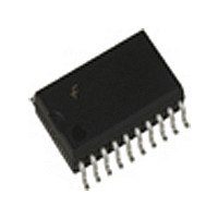
74ACT574SCX Fairchild Semiconductor, 74ACT574SCX Datasheet - Page 2

74ACT574SCX
Manufacturer Part Number
74ACT574SCX
Description
IC FLIP FLOP OCTAL D 3ST 20SOIC
Manufacturer
Fairchild Semiconductor
Series
74ACTr
Type
D-Type Busr
Datasheet
1.74ACT574SCX.pdf
(9 pages)
Specifications of 74ACT574SCX
Function
Standard
Output Type
Tri-State Non Inverted
Number Of Elements
1
Number Of Bits Per Element
8
Frequency - Clock
110MHz
Delay Time - Propagation
7ns
Trigger Type
Positive Edge
Current - Output High, Low
24mA, 24mA
Voltage - Supply
4.5 V ~ 5.5 V
Operating Temperature
-40°C ~ 85°C
Mounting Type
Surface Mount
Package / Case
20-SOIC (7.5mm Width)
Logic Family
ACT
Technology
CMOS
Number Of Bits
8
Number Of Elements
1
Clock-edge Trigger Type
Positive-Edge
Polarity
Non-Inverting
Operating Supply Voltage (typ)
5V
Package Type
SOIC W
Propagation Delay Time
12ns
Low Level Output Current
24mA
High Level Output Current
-24mA
Frequency (max)
85MHz
Operating Supply Voltage (min)
4.5V
Operating Supply Voltage (max)
5.5V
Operating Temp Range
-40C to 85C
Operating Temperature Classification
Industrial
Mounting
Surface Mount
Pin Count
20
Lead Free Status / RoHS Status
Lead free / RoHS Compliant
Available stocks
Company
Part Number
Manufacturer
Quantity
Price
Part Number:
74ACT574SCX
Manufacturer:
FSC
Quantity:
20 000
www.fairchildsemi.com
Logic Symbols
Connection Diagram
Logic Diagram
Please note that this diagram is provided only for the understanding of logic operations and should not be used to estimate propagation delays.
IEEE/IEC
2
Pin Descriptions
Function Table
H
L
X
Z
NC
Functional Description
The AC/ACT574 consists of eight edge-triggered flip-flops
with individual D-type inputs and 3-STATE true outputs.
The buffered clock and buffered Output Enable are com-
mon to all flip-flops. The eight flip-flops will store the state
of their individual D-type inputs that meet the setup and
hold time requirements on the LOW-to-HIGH Clock (CP)
transition. With the Output Enable (OE) LOW, the contents
of the eight flip-flops are available at the outputs. When OE
is HIGH, the outputs go to the high impedance state. Oper-
ation of the OE input does not affect the state of the flip-
flops.
D
CP
OE
O
OE
0
0
LOW Voltage Level
High Impedance
H
H
H
H
HIGH Voltage Level
Immaterial
L
L
L
L
Pin Names
–D
–O
LOW-to-HIGH Transition
No Change
Inputs
7
7
CP D
H
H
H
H
H
H
H
H
L
L
L
L
Internal
Data Inputs
Clock Pulse Input
3-STATE Output Enable Input
3-STATE Outputs
NC
NC
NC
NC
Q
H
H
L
L
Outputs
NC
O
NC
H
Z
Z
Z
Z
L
N
Description
Hold
Hold
Load
Load
Data Available
Data Available
No Change in Data
No Change in Data
Function


