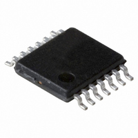
74LV74PW,118 NXP Semiconductors, 74LV74PW,118 Datasheet - Page 2

74LV74PW,118
Manufacturer Part Number
74LV74PW,118
Description
IC DUAL D FF POSEDG TRIG 14TSSOP
Manufacturer
NXP Semiconductors
Series
74LVr
Type
D-Typer
Specifications of 74LV74PW,118
Output Type
Differential
Package / Case
14-TSSOP
Function
Set(Preset) and Reset
Number Of Elements
2
Number Of Bits Per Element
1
Frequency - Clock
56MHz
Trigger Type
Positive Edge
Current - Output High, Low
12mA, 12mA
Voltage - Supply
1 V ~ 5.5 V
Operating Temperature
-40°C ~ 125°C
Mounting Type
Surface Mount
Number Of Circuits
2
Logic Family
LV
Logic Type
D-Type Edge Triggered Flip-Flop
Polarity
Inverting/Non-Inverting
Input Type
Single-Ended
Propagation Delay Time
11 ns at 3.3 V
High Level Output Current
- 12 mA
Low Level Output Current
12 mA
Supply Voltage (max)
5.5 V
Maximum Operating Temperature
+ 125 C
Mounting Style
SMD/SMT
Minimum Operating Temperature
- 40 C
Supply Voltage (min)
1 V
Delay Time - Propagation
-
Technology
CMOS
Number Of Bits
2
Number Of Elements
2
Clock-edge Trigger Type
Positive-Edge
Operating Supply Voltage (typ)
3.3V
Package Type
TSSOP
Frequency (max)
56MHz
Operating Supply Voltage (min)
1V
Operating Supply Voltage (max)
5.5V
Operating Temp Range
-40C to 125C
Operating Temperature Classification
Automotive
Mounting
Surface Mount
Pin Count
14
Lead Free Status / RoHS Status
Lead free / RoHS Compliant
Delay Time - Propagation
-
Lead Free Status / Rohs Status
Lead free / RoHS Compliant
Other names
74LV74PW-T
74LV74PW-T
935175140118
74LV74PW-T
935175140118
1. C
2. The condition is V
Philips Semiconductors
FEATURES
QUICK REFERENCE DATA
GND = 0V; T
NOTES:
ORDERING INFORMATION
PIN DESCRIPTION
t
f
C
C
14-Pin Plastic DIL
14-Pin Plastic SO
14-Pin Plastic SSOP Type II
14-Pin Plastic TSSOP Type I
1, 13
2, 12
3, 11
4, 10
5, 9
6, 8
7
14
1998 Apr 20
PHL
max
Wide operating voltage: 1.0 to 5.5V
Optimized for Low Voltage applications: 1.0 to 3.6V
Accepts TTL input levels between V
Typical V
T
Typical V
T
Output capability: standard
I
Dual D-type flip-flop with set and reset;
positive edge-trigger
I
PD
CC
NUMBER
P
f
f
S (C
amb
amb
i
o
PD
D
= input frequency in MHz; C
SYMBOL
/t
= output frequency in MHz; V
category: flip-flops
PIN
PLH
= C
= 25 C
= 25 C
L
is used to determine the dynamic power dissipation (P
PD
OLP
OHV
V
amb
PACKAGES
CC
(output ground bounce) t 0.8V @ V
(output V
V
2
= 25 C; t
CC
SYMBOL
1CP, 2CP
1R
1S
1Q, 2Q
1D, 2D
1Q
2
GND
f
I
V
D,
D,
Propagation delay
nCP to nQ, nQ
nS
nR
Maximum clock frequency
Input capacitance
Power dissipation capacitance per flip-flop
o
x f
= GND to V
) = sum of the outputs.
,
CC
2R
2S
2Q
D
D
i
OH
r
)S (C
to nQ, nQ
to nQ, nQ
D
D
=t
undershoot) u 2V @ V
f
v2.5 ns
Asynchronous reset-direct input
(active-LOW)
Data inputs
Clock input (LOW-to-HIGH),
edge-triggered)
Asynchronous set-direct input
(active-LOW)
True flip-flop outputs
Complement flip-flop outputs
Ground (0V)
Positive supply voltage
L
L
CC
= output load capacitance in pF;
CC
PARAMETER
V
CC
= supply voltage in V;
CC
TEMPERATURE RANGE
2
= 2.7V and V
–40 C to +125 C
–40 C to +125 C
–40 C to +125 C
–40 C to +125 C
FUNCTION
f
o
) where:
CC
CC
CC
= 3.3V,
= 3.3V,
= 3.6V
D
in W)
C
V
C
V
Notes 1 and 2
OUTSIDE NORTH AMERICA
CC
CC
L
L
= 15pF
= 15pF
2
= 3.3V
= 3.3V
DESCRIPTION
The 74LV74 is a low-voltage Si-gate CMOS device and is pin and
function compatible with 74HC/HCT74.
The 74LV74 is a dual positive edge triggered, D-type flip-flop with
individual data (D) inputs, clock (CP) inputs, set (S
inputs; also complementary Q and Q outputs.
The set and reset are asynchronous active LOW inputs and operate
independently of the clock input. Information on the data input is
transferred to the Q output on the LOW-to-HIGH transition of the
clock pulse. The D inputs must be stable one set-up time prior to the
LOW-to-HIGH clock transition, for predictable operation.
Schmitt-trigger action in the clock input makes the circuit highly
tolerant to slower clock rise and fall times.
FUNCTION TABLE
H
L
X
°
Q
74LV74 PW
n+1
CONDITIONS
74LV74 DB
74LV74 N
74LV74 D
S
S
H
H
H
L
L
D
D
= HIGH voltage level
= LOW voltage level
= don’t care
= LOW-to-HIGH CP transition
= state after the next LOW-to-HIGH CP transition
R
R
H
H
H
L
L
INPUTS
INPUTS
D
D
NORTH AMERICA
CP
CP
X
X
X
°
°
74LV74PW DH
74LV74 DB
74LV74 N
74LV74 D
TYPICAL
3.5
14
14
76
24
11
D
X
X
X
D
H
L
Product specification
Q
Q
H
H
H
L
n+1
L
OUTPUTS
OUTPUTS
D
PKG. DWG. #
853-1888 19258
) and (R
74LV74
SOT108-1
SOT337-1
SOT402-1
SOT27-1
UNIT
MHz
ns
pF
pF
Q
D
)
Q
H
H
H
L
n+1
L


