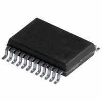
74ABT823DB,112 NXP Semiconductors, 74ABT823DB,112 Datasheet - Page 7

74ABT823DB,112
Manufacturer Part Number
74ABT823DB,112
Description
IC 9BIT D-TYPE F-F 3-ST 24SSOP
Manufacturer
NXP Semiconductors
Series
74ABTr
Type
D-Type Busr
Datasheet
1.74ABT827D602.pdf
(17 pages)
Specifications of 74ABT823DB,112
Function
Master Reset
Output Type
Tri-State Non Inverted
Number Of Elements
1
Number Of Bits Per Element
9
Frequency - Clock
200MHz
Delay Time - Propagation
4.3ns
Trigger Type
Positive Edge
Current - Output High, Low
32mA, 64mA
Voltage - Supply
4.5 V ~ 5.5 V
Operating Temperature
-40°C ~ 85°C
Mounting Type
Surface Mount
Package / Case
24-SSOP
Lead Free Status / RoHS Status
Lead free / RoHS Compliant
Other names
74ABT823DB
74ABT823DB
935069200112
74ABT823DB
935069200112
NXP Semiconductors
Table 6.
[1]
[2]
[3]
[4]
10. Dynamic characteristics
Table 7.
GND = 0 V; for test circuit, see
74ABT823_3
Product data sheet
Symbol
ΔI
C
C
Symbol Parameter
f
t
t
t
t
t
t
t
t
t
t
t
max
PLH
PHL
PZH
PZL
PHZ
PLZ
su(H)
su(L)
h(H)
h(L)
WH
I
O
CC
For valid test results, data must not be loaded into the flip-flops (or latches) after applying the power.
This parameter is valid for any V
a transition time of up to 100 μs is permitted.
Not more than one output should be tested at a time, and the duration of the test should not exceed one second.
This is the increase in supply current for each input at 3.4 V.
maximum
frequency
LOW to HIGH
propagation delay
HIGH to LOW
propagation delay
OFF-state to HIGH
propagation delay
OFF-state to LOW
propagation delay
HIGH to OFF-state
propagation delay
LOW to OFF-state
propagation delay
set-up time HIGH
set-up time LOW
hold time HIGH
hold time LOW
pulse width HIGH
Parameter
additional supply
current
input capacitance
output capacitance
Static characteristics
Dynamic characteristics
Figure
Conditions
see
CP to Qn, see
CP to Qn, see
MR to Qn, see
OE to Qn; see
OE to Qn; see
OE to Qn; see
OE to Qn; see
Dn to CP; see
CE to CP; see
Dn to CP; see
CE to CP; see
CP to Dn; see
CP to CE; see
CP to Dn; see
CP to CE; see
CP; see
CC
…continued
Conditions
per input pin; V
one input at 3.4 V;
other inputs at V
V
outputs disabled; V
between 0 V and 2.1 V, with a transition time of up to 10 ms. From V
Figure 5
I
9.
= 0 V or V
Figure 5
All information provided in this document is subject to legal disclaimers.
Figure 7
Figure 7
Figure 7
Figure 7
Figure 5
Figure 5
Figure 8
Figure 8
Figure 8
Figure 8
Figure 7
Figure 7
Figure 7
Figure 7
Figure 6
CC
Rev. 03 — 23 March 2010
CC
CC
= 5.5 V;
O
or GND
= 0 V or V
9-bit D-type flip-flop with reset and enable; 3-state
CC
[4]
25 °C; V
+2.0 −0.5
+1.0 −1.4
+1.3 −0.3
Min
125
2.1
2.2
2.0
1.0
2.2
2.7
2.5
2.1
2.1
3.3
1.3
2.0
2.9
Min
-
-
-
Typ
200
4.3
4.4
4.1
3.0
4.1
4.8
5.0
0.5
0.2
1.5
0.0
0.7
1.9
25 °C
CC
Typ
0.5
4
7
= 5.0 V −40 °C to +85 °C;
Max
5.9
6.1
6.3
4.5
5.6
6.2
6.4
-
-
-
-
-
-
-
-
-
-
Max
1.5
-
-
CC
V
CC
= 2.1 V to V
−40 °C to +85 °C Unit
+2.0
+1.0
+1.3
Min
74ABT823
125
2.1
2.2
2.0
1.0
2.2
2.7
2.5
2.1
2.1
3.3
1.3
2.0
2.9
Min
= 5.0 V ± 0.5 V
-
-
-
© NXP B.V. 2010. All rights reserved.
CC
Max
Max
6.8
6.7
7.1
5.3
6.3
6.9
6.9
1.5
-
-
-
-
-
-
-
-
-
-
= 5 V ± 10 %
-
-
7 of 17
mA
pF
pF
Unit
MHz
ns
ns
ns
ns
ns
ns
ns
ns
ns
ns
ns
ns
ns
ns
ns
ns


