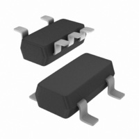
74AHC1G14GV,125 NXP Semiconductors, 74AHC1G14GV,125 Datasheet - Page 7

74AHC1G14GV,125
Manufacturer Part Number
74AHC1G14GV,125
Description
IC SCHMITT-TRG INV GATE SOT-753
Manufacturer
NXP Semiconductors
Series
74AHCr
Datasheet
1.74AHC1G14GV125.pdf
(15 pages)
Specifications of 74AHC1G14GV,125
Number Of Circuits
1
Logic Type
Inverter with Schmitt Trigger
Package / Case
SC-74-5, SOT-753
Number Of Inputs
1
Current - Output High, Low
8mA, 8mA
Voltage - Supply
2 V ~ 5.5 V
Operating Temperature
-40°C ~ 125°C
Mounting Type
Surface Mount
Logic Family
74AHC
High Level Output Current
- 8 mA
Low Level Output Current
8 mA
Propagation Delay Time
16.5 ns
Supply Voltage (max)
5.5 V
Supply Voltage (min)
2 V
Maximum Operating Temperature
+ 125 C
Minimum Operating Temperature
- 40 C
Mounting Style
SMD/SMT
Operating Supply Voltage
2 V to 5.5 V
Logical Function
Inverter Schmit Trig
Number Of Elements
1
Input Type
Schmitt Trigger
Operating Supply Voltage (typ)
5V
Package Type
SOT
Operating Temp Range
-40C to 125C
Pin Count
5
Quiescent Current
1uA
Output Type
Schmitt Trigger
Technology
CMOS
Mounting
Surface Mount
Operating Temperature Classification
Automotive
Operating Supply Voltage (max)
5.5V
Operating Supply Voltage (min)
2V
Lead Free Status / RoHS Status
Lead free / RoHS Compliant
Lead Free Status / RoHS Status
Lead free / RoHS Compliant, Lead free / RoHS Compliant
Other names
568-2256-2
74AHC1G14GV
935271665125
74AHC1G14GV
935271665125
Available stocks
Company
Part Number
Manufacturer
Quantity
Price
Company:
Part Number:
74AHC1G14GV,125
Manufacturer:
NXP Semiconductors
Quantity:
4 750
NXP Semiconductors
13. Waveforms
Table 10.
74AHC_AHCT1G14_6
Product data sheet
Type number
74AHC1G14
74AHCT1G14
Fig 5. The input (A) to output (Y) propagation delays
Fig 7. Transfer characteristic
Y output
A input
The test data is given in
Test data
V
O
13.1 Transfer characteristic waveforms
V
V
M
T
V
M
t
V
PHL
H
Table 10
Input
V
GND to V
GND to 3.0 V
V
I
T+
mna026
CC
V
I
t
PLH
mna033
Rev. 06 — 18 May 2009
74AHC1G14; 74AHCT1G14
V
0.5 V
1.5 V
Fig 6. Load circuitry for switching times
Fig 8.
M
CC
GENERATOR
Test data is given in
Definitions for test circuit:
C
R
impedance Z
The definitions of V
PULSE
L
T
V
V
= Load capacitance.
= Termination resistance should be equal to output
O
I
V
T+
o
of the pulse generator.
V
I
Table
R T
T+
Output
V
0.5 V
0.5 V
V
9.
Inverting Schmitt trigger
M
, V
T
DUT
V
CC
T
CC
CC
and V
V
© NXP B.V. 2009. All rights reserved.
O
mna027
H
V
H
C L
mna101
7 of 15


