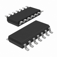
74LVCU04AD,118 NXP Semiconductors, 74LVCU04AD,118 Datasheet - Page 2

74LVCU04AD,118
Manufacturer Part Number
74LVCU04AD,118
Description
IC HEX INVERTER 14-SOIC
Manufacturer
NXP Semiconductors
Series
74LVCUr
Datasheet
1.74LVCU04ABQ115.pdf
(17 pages)
Specifications of 74LVCU04AD,118
Number Of Circuits
6
Logic Type
Inverter
Package / Case
14-SOIC (3.9mm Width), 14-SOL
Number Of Inputs
1
Current - Output High, Low
24mA, 24mA
Voltage - Supply
2.7 V ~ 3.6 V
Operating Temperature
-40°C ~ 125°C
Mounting Type
Surface Mount
Logic Family
74LVC
High Level Output Current
- 24 mA
Low Level Output Current
24 mA
Propagation Delay Time
5 ns
Supply Voltage (max)
3.6 V
Supply Voltage (min)
1.2 V
Maximum Operating Temperature
+ 125 C
Minimum Operating Temperature
- 40 C
Mounting Style
SMD/SMT
Operating Supply Voltage
1.2 V to 3.6 V
Lead Free Status / RoHS Status
Lead free / RoHS Compliant
Lead Free Status / RoHS Status
Lead free / RoHS Compliant, Lead free / RoHS Compliant
Other names
568-2308-2
74LVCU04AD-T
935260740118
74LVCU04AD-T
935260740118
Available stocks
Company
Part Number
Manufacturer
Quantity
Price
Part Number:
74LVCU04AD,118
Manufacturer:
NEXPERIA/安世
Quantity:
20 000
Philips Semiconductors
FEATURES
QUICK REFERENCE DATA
GND = 0 V; t
Notes
1. C
2. The condition is V
FUNCTION TABLE
See note 1.
Note
1. H = HIGH voltage level;
2004 Mar 12
t
C
C
PHL
Wide supply voltage range from 1.2 V to 3.6 V
Inputs accept voltages up to 5.5 V
CMOS low-power consumption
Direct interface with TTL levels
In accordance with JEDEC standard no. 8-1A
ESD protection:
HBM EIA/JESD22-A114-A exceeds 2000 V
MM EIA/JESD22-A115-A exceeds 200 V.
Specified from 40 C to +85 C and
I
PD
Hex inverter
40 C to +125 C.
SYMBOL
P
f
f
C
V
N = total load switching outputs;
L = LOW voltage level.
i
o
/t
(C
D
CC
PD
= input frequency in MHz;
L
PLH
= output frequency in MHz;
= output load capacitance in pF;
= C
L
is used to determine the dynamic power dissipation (P
= supply voltage in Volts;
PD
V
CC
r
= t
2
V
f
CC
propagation delay nA to nY
input capacitance
power dissipation capacitance per gate
f
o
2.5 ns; T
2
) = sum of the outputs.
I
f
= GND to V
i
INPUT
N + (C
nA
amb
H
L
PARAMETER
= 25 C.
L
CC
.
V
CC
2
f
o
) where:
2
C
notes 1 and 2
DESCRIPTION
The 74LVCU04A is a high-performance, low-power,
low-voltage, Si-gate CMOS device and superior to most
advanced CMOS compatible TTL families.
The 74LVCU04A is a general purpose hex inverter. Each
of the six inverters is a single stage with unbuffered
outputs.
L
D
= 50 pF; V
in W).
CONDITIONS
CC
= 3.3 V
OUTPUT
nY
H
L
2.1
5.5
8.5
TYPICAL
Product specification
74LVCU04A
ns
pF
pF
UNIT


