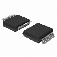
74HC259DB,112 NXP Semiconductors, 74HC259DB,112 Datasheet - Page 11

74HC259DB,112
Manufacturer Part Number
74HC259DB,112
Description
IC 8BIT ADDRESSABLE LATCH 16SSOP
Manufacturer
NXP Semiconductors
Series
74HCr
Datasheets
1.74HCT4046ADB112.pdf
(19 pages)
2.74HCT4046ADB112.pdf
(23 pages)
3.74HCT259N652.pdf
(11 pages)
Specifications of 74HC259DB,112
Logic Type
D-Type, Addressable
Package / Case
16-SSOP
Circuit
1:8
Output Type
Standard
Voltage - Supply
2 V ~ 6 V
Independent Circuits
1
Delay Time - Propagation
17ns
Current - Output High, Low
5.2mA, 5.2mA
Operating Temperature
-40°C ~ 125°C
Mounting Type
Surface Mount
Number Of Circuits
1
Logic Family
HC
Polarity
Non-Inverting
High Level Output Current
- 5.2 mA
Low Level Output Current
5.2 mA
Propagation Delay Time
18 ns at 5 V
Supply Voltage (max)
6 V
Supply Voltage (min)
2 V
Maximum Operating Temperature
+ 125 C
Minimum Operating Temperature
- 40 C
Mounting Style
SMD/SMT
Lead Free Status / RoHS Status
Lead free / RoHS Compliant
Lead Free Status / RoHS Status
Lead free / RoHS Compliant, Lead free / RoHS Compliant
Other names
568-2657-5
935187410112
935187410112
Philips Semiconductors
PACKAGE OUTLINES
See
December 1990
8-bit addressable latch
(1) HC : V
The shaded areas indicate when the input is
permitted to change for predictable output
performance.
(1) HC : V
The shaded areas indicate when the input is
permitted to change for predictable output
performance.
(1) HC : V
“74HC/HCT/HCU/HCMOS Logic Package Outlines”
HCT: V
HCT: V
HCT: V
M
M
M
M
M
M
Fig.9 Waveforms showing the conditional reset input (MR) to output (Q
= 50%; V
= 50%; V
= 50%; V
= 1.3 V; V
= 1.3 V; V
= 1.3 V; V
Fig.11 Waveforms showing the address set-up and hold times for A
Fig.10 Waveforms showing the data set-up and hold times for the D input to LE input.
I
I
I
I
I
I
= GND to V
= GND to V
= GND to V
= GND to 3 V.
= GND to 3 V.
= GND to 3 V.
CC
CC
CC
.
.
.
.
11
n
n
) propagation delays.
inputs to LE input.
74HC/HCT259
Product specification


