74LV573N,112 NXP Semiconductors, 74LV573N,112 Datasheet
74LV573N,112
Specifications of 74LV573N,112
935060100112


Related parts for 74LV573N,112


74LV573N,112 Summary of contents
Page 1
Octal D-type transparent latch; 3-state Rev. 03 — 15 April 2009 1. General description The 74LV573 is a low-voltage Si-gate CMOS device that is pin and function compatible with 74HC573 and 74HCT573. The 74LV573 consists of eight D-type transparent ...
Page 2
... NXP Semiconductors 3. Ordering information Table 1. Ordering information Type number Package Temperature range Name 74LV573N +125 C 74LV573D +125 C 74LV573DB +125 C 74LV573PW +125 C 4. Functional diagram Fig 1. Logic symbol 74LV573_3 Product data sheet Description DIP20 plastic dual in-line package; 20 leads (300 mil) SO20 plastic small outline package ...
Page 3
... NXP Semiconductors Fig 3. Functional diagram LATCH LATCH Fig 4. Logic diagram 74LV573_3 Product data sheet LATCH OUTPUTS LATCH LATCH Rev. 03 — 15 April 2009 Octal D-type transparent latch; 3-state 3-STATE mna809 LATCH LATCH LATCH 74LV573 LATCH mna810 © NXP B.V. 2009. All rights reserved. ...
Page 4
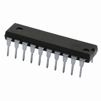
... NXP Semiconductors 5. Pinning information 5.1 Pinning 74LV573 GND 001aaj966 Fig 5. Pin configuration DIP20, SO20 5.2 Pin description Table 2. Pin description Symbol Pin GND 19, 18, 17, 16, 15, 14, 13 Functional description [1] Table 3. Functional table Operating modes Enable and read register (transparent mode) Latch and read register ...
Page 5
... NXP Semiconductors 7. Limiting values Table 4. Limiting values In accordance with the Absolute Maximum Rating System (IEC 60134). Voltages are referenced to GND (ground = 0 V). Symbol Parameter V supply voltage CC I input clamping current IK I output clamping current OK I output current O I supply current CC I ground current ...
Page 6
... NXP Semiconductors 9. Static characteristics Table 6. Static characteristics At recommended operating conditions. Voltages are referenced to GND (ground = 0 V). Symbol Parameter V HIGH-level input voltage IH V LOW-level input voltage IL V HIGH-level output voltage OH V LOW-level output voltage OL I input leakage current I I OFF-state output current ...
Page 7
... NXP Semiconductors 10. Dynamic characteristics Table 7. Dynamic characteristics Voltages are referenced to GND (ground = 0 V). For test circuit see Symbol Parameter Conditions t propagation delay Dn to Qn; see Qn; see enable time OE to Qn; see disable time OE to Qn; see dis pulse width LE HIGH; see set-up time nD to nCP; see ...
Page 8
... NXP Semiconductors Table 7. Dynamic characteristics Voltages are referenced to GND (ground = 0 V). For test circuit see Symbol Parameter Conditions t hold time Dn to LE; see power dissipation capacitance V = GND [1] All typical values are measured the same as t and PLH PHL t is the same as t and t ...
Page 9
... NXP Semiconductors LE input Qn output Measurement points are given in V and V are typical voltage output levels that occur with the output load Fig 8. Latch Enable input (LE) pulse width, the latch enable input to output (Qn) propagation delays OE input Qn output LOW-to-OFF OFF-to-LOW Qn output HIGH-to-OFF OFF-to-HIGH ...
Page 10
... NXP Semiconductors Dn input LE input Measurement points are given in V and V are typical voltage output levels that occur with the output load Fig 10. Data set-up and hold times for the Dn input to the LE input Table 8. Measurement points Supply voltage Input < 2.7 V 0. ...
Page 11
... NXP Semiconductors Test data is given in Table Definitions for test circuit Load resistance Load capacitance including jig and probe capacitance Termination resistance should be equal to output impedance External voltage for measuring switching times. EXT Fig 11. Test circuit for measuring switching times Table 9. Test data ...
Page 12
... NXP Semiconductors 12. Package outline DIP20: plastic dual in-line package; 20 leads (300 mil pin 1 index 1 DIMENSIONS (inch dimensions are derived from the original mm dimensions UNIT max. min. max. mm 4.2 0.51 3.2 inches 0.17 0.02 0.13 Note 1. Plastic or metal protrusions of 0.25 mm (0.01 inch) maximum per side are not included. ...
Page 13
... NXP Semiconductors SO20: plastic small outline package; 20 leads; body width 7 pin 1 index 1 e DIMENSIONS (inch dimensions are derived from the original mm dimensions) A UNIT max. 0.3 2.45 2.65 mm 0.25 0.1 2.25 0.012 0.096 0.1 inches 0.01 0.004 0.089 Note 1. Plastic or metal protrusions of 0.15 mm (0.006 inch) maximum per side are not included. ...
Page 14
... NXP Semiconductors SSOP20: plastic shrink small outline package; 20 leads; body width 5 pin 1 index 1 e DIMENSIONS (mm are the original dimensions) A UNIT max. 0.21 1. 0.25 0.05 1.65 Note 1. Plastic or metal protrusions of 0.2 mm maximum per side are not included. OUTLINE VERSION IEC SOT339-1 Fig 14. Package outline SOT339-1 (SSOP20) ...
Page 15
... NXP Semiconductors TSSOP20: plastic thin shrink small outline package; 20 leads; body width 4 pin 1 index 1 DIMENSIONS (mm are the original dimensions) A UNIT max. 0.15 0.95 mm 1.1 0.25 0.05 0.80 Notes 1. Plastic or metal protrusions of 0.15 mm maximum per side are not included. 2. Plastic interlead protrusions of 0.25 mm maximum per side are not included. ...
Page 16
... Document ID Release date 74LV573_3 20090415 • Modifications: The format of this data sheet has been redesigned to comply with the new identity guidelines of NXP Semiconductors. • Legal texts have been adapted to the new company name when appropriate. 74LV573_2 19980610 74LV573_1 19970606 74LV573_3 Product data sheet Octal D-type transparent latch ...
Page 17
... Right to make changes — NXP Semiconductors reserves the right to make changes to information published in this document, including without limitation specifications and product descriptions, at any time and without notice ...
Page 18
... NXP Semiconductors 17. Contents 1 General description . . . . . . . . . . . . . . . . . . . . . . 1 2 Features . . . . . . . . . . . . . . . . . . . . . . . . . . . . . . . 1 3 Ordering information . . . . . . . . . . . . . . . . . . . . . 2 4 Functional diagram . . . . . . . . . . . . . . . . . . . . . . 2 5 Pinning information . . . . . . . . . . . . . . . . . . . . . . 4 5.1 Pinning . . . . . . . . . . . . . . . . . . . . . . . . . . . . . . . 4 5.2 Pin description . . . . . . . . . . . . . . . . . . . . . . . . . 4 6 Functional description . . . . . . . . . . . . . . . . . . . 4 7 Limiting values Recommended operating conditions Static characteristics Dynamic characteristics . . . . . . . . . . . . . . . . . . 7 11 Waveforms . . . . . . . . . . . . . . . . . . . . . . . . . . . . . 8 12 Package outline . . . . . . . . . . . . . . . . . . . . . . . . 12 13 Abbreviations . . . . . . . . . . . . . . . . . . . . . . . . . . 16 14 Revision history ...