HSTL16919DGG,112 NXP Semiconductors, HSTL16919DGG,112 Datasheet - Page 4
HSTL16919DGG,112
Manufacturer Part Number
HSTL16919DGG,112
Description
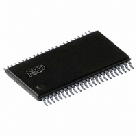
IC MEMORY ADDRESS LATCH 48TSSOP
Manufacturer
NXP Semiconductors
Series
HSTLr
Datasheet
1.HSTL16919DGG112.pdf
(8 pages)
Specifications of HSTL16919DGG,112
Logic Type
D-Type, Addressable
Circuit
9:18
Output Type
Standard
Voltage - Supply
3.15 V ~ 3.45 V
Independent Circuits
1
Delay Time - Propagation
1.9ns
Current - Output High, Low
24mA, 24mA
Operating Temperature
0°C ~ 70°C
Mounting Type
Surface Mount
Package / Case
48-TSSOP
Lead Free Status / RoHS Status
Lead free / RoHS Compliant
Other names
935270254112
HSTL16919DGG
HSTL16919DGG
HSTL16919DGG
HSTL16919DGG


1. Stresses beyond those listed may cause permanent damage to the device. These are stress ratings only and functional operation of the
2. The input and output negative-voltage ratings may be exceeded if the input and output clamp-current ratings are observed.
3. This current flows only when the output is in the high state and V
4. The package thermal impedance is calculated in accordance with JESD 51.
1. All unused inputs of the device must be held at V
Philips Semiconductors
ABSOLUTE MAXIMUM RATINGS
Over operating free-air temperature range (unless otherwise noted).
NOTES:
RECOMMENDED OPERATING CONDITIONS
NOTE:
2001 Jul 19
SYMBOL
SYMBOL
SYMBOL
9-bit to 18-bit HSTL to LVTTL memory address latch
with 12k ohm pull-up resistor
device at these or any other conditions beyond those indicated under “recommended operating conditions” is not implied. Exposure to
absolute-maximum-rated conditions for extended periods may affect device reliability.
V
T
V
V
T
I
V
V
I
V
V
V
I
I
REF
amb
V
OK
I
V
OH
OL
CC
IK
stg
CC
O
JA
IH
IH
IL
IL
O
I
I
Supply voltage range
Input voltage range
Output voltage range
Input clamp current
Output clamp current
Continuous output current
Continuous current through each V
Package thermal impedance
Storage temperature range
Supply voltage
Reference voltage
Input voltage
AC high-level input voltage
AC low-level input voltage
DC high-level input voltage
DC low-level input voltage
High-level output current
Low-level output current
Operating free-air temperature range
PARAMETER
2
2
3
PARAMETER
PARAMETER
1
4
CC
CC
or GND
or GND to ensure proper device operation.
1
All inputs
All inputs
All inputs
All inputs
O
> V
4
CC
V
.
O
CONDITIONS
V
< 0 or V
O
V
V
= 0 to V
REF
REF
V
I
< 0
3.15
0.68
Min
+ 200 mV
+ 100 mV
O
—
—
—
—
0
0
> V
CC
CC
LIMITS
Nom
0.75
—
—
—
—
—
—
—
—
—
–0.5 to V
–0.5 to V
–0.5 to +4.6
–65 to +150
RATING
V
V
REF
REF
–50
100
89
50
50
CC
CC
Max
3.45
– 200 mV
– 100 mV
–24
+70
0.9
1.5
—
—
24
HSTL16919
+0.5
+0.5
Product data
UNIT
UNIT
UNIT
mA
mA
mA
mA
C/W
mA
mA
V
V
V
V
V
V
V
V
V
V
C
C
Related parts for HSTL16919DGG,112
Image
Part Number
Description
Manufacturer
Datasheet
Request
R

Part Number:
Description:
Hstl16919 9-bit To 18-bit Hstl To Lvttl Memory Address Latch With 12 Kohm Pull-up Resistor
Manufacturer:
NXP Semiconductors
Datasheet:
Part Number:
Description:
NXP Semiconductors designed the LPC2420/2460 microcontroller around a 16-bit/32-bitARM7TDMI-S CPU core with real-time debug interfaces that include both JTAG andembedded trace
Manufacturer:
NXP Semiconductors
Datasheet:

Part Number:
Description:
NXP Semiconductors designed the LPC2458 microcontroller around a 16-bit/32-bitARM7TDMI-S CPU core with real-time debug interfaces that include both JTAG andembedded trace
Manufacturer:
NXP Semiconductors
Datasheet:
Part Number:
Description:
NXP Semiconductors designed the LPC2468 microcontroller around a 16-bit/32-bitARM7TDMI-S CPU core with real-time debug interfaces that include both JTAG andembedded trace
Manufacturer:
NXP Semiconductors
Datasheet:
Part Number:
Description:
NXP Semiconductors designed the LPC2470 microcontroller, powered by theARM7TDMI-S core, to be a highly integrated microcontroller for a wide range ofapplications that require advanced communications and high quality graphic displays
Manufacturer:
NXP Semiconductors
Datasheet:
Part Number:
Description:
NXP Semiconductors designed the LPC2478 microcontroller, powered by theARM7TDMI-S core, to be a highly integrated microcontroller for a wide range ofapplications that require advanced communications and high quality graphic displays
Manufacturer:
NXP Semiconductors
Datasheet:
Part Number:
Description:
The Philips Semiconductors XA (eXtended Architecture) family of 16-bit single-chip microcontrollers is powerful enough to easily handle the requirements of high performance embedded applications, yet inexpensive enough to compete in the market for hi
Manufacturer:
NXP Semiconductors
Datasheet:
Part Number:
Description:
The XA-S3 device is a member of Philips Semiconductors? XA(eXtended Architecture) family of high performance 16-bitsingle-chip microcontrollers
Manufacturer:
NXP Semiconductors
Datasheet:

Part Number:
Description:
The NXP BlueStreak LH75401/LH75411 family consists of two low-cost 16/32-bit System-on-Chip (SoC) devices
Manufacturer:
NXP Semiconductors
Datasheet:
Part Number:
Description:
The NXP LPC3130/3131 combine an 180 MHz ARM926EJ-S CPU core, high-speed USB2
Manufacturer:
NXP Semiconductors
Datasheet:
Part Number:
Description:
The NXP LPC3141 combine a 270 MHz ARM926EJ-S CPU core, High-speed USB 2
Manufacturer:
NXP Semiconductors
Part Number:
Description:
The NXP LPC3143 combine a 270 MHz ARM926EJ-S CPU core, High-speed USB 2
Manufacturer:
NXP Semiconductors

Part Number:
Description:
The NXP LPC3152 combines an 180 MHz ARM926EJ-S CPU core, High-speed USB 2
Manufacturer:
NXP Semiconductors
Part Number:
Description:
The NXP LPC3154 combines an 180 MHz ARM926EJ-S CPU core, High-speed USB 2
Manufacturer:
NXP Semiconductors