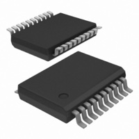
CBT3244ADB,118 NXP Semiconductors, CBT3244ADB,118 Datasheet - Page 6

CBT3244ADB,118
Manufacturer Part Number
CBT3244ADB,118
Description
IC BUS SWITCH OCTAL 8BIT 20SSOP
Manufacturer
NXP Semiconductors
Series
74CBTr
Type
Bus Switchr
Datasheet
1.CBT3244ADB118.pdf
(18 pages)
Specifications of CBT3244ADB,118
Circuit
4 x 1:1
Independent Circuits
2
Current - Output High, Low
15mA, 64mA
Voltage Supply Source
Single Supply
Voltage - Supply
4.5 V ~ 5.5 V
Operating Temperature
-40°C ~ 85°C
Mounting Type
Surface Mount
Package / Case
20-SSOP
Lead Free Status / RoHS Status
Lead free / RoHS Compliant
Other names
935276001118
CBT3244ADB-T
CBT3244ADB-T
CBT3244ADB-T
CBT3244ADB-T
Philips Semiconductors
9. Static characteristics
Table 6:
T
[1]
[2]
[3]
10. Dynamic characteristics
Table 7:
T
[1]
[2]
[3]
9397 750 13362
Product data sheet
Symbol
V
I
I
C
C
R
Symbol
t
t
t
LI
CC
PD
en
dis
amb
amb
I
IK
i
io
on
CC
[3]
All typical values are at V
This is the increase in supply current for each input that is at the specified TTL voltage level rather than V
Measured by the voltage drop between the A and the B terminals at the indicated current through the switch. ON-state resistance is
determined by the lowest voltage of the two (A or B) terminals.
This parameter is warranted but not production tested. The propagation delay is based on the RC time constant of the typical ON-state
resistance of the switch and a load capacitance of 50 pF, when driven by an ideal voltage source (zero output impedance).
Output enable time to HIGH and LOW level.
Output disable time from HIGH and LOW level.
= 40 C to +85 C
[2]
= 40 C to +85 C; V
Parameter
input clamping voltage
input leakage current
quiescent supply current
additional quiescent supply current
(per input)
input capacitance (control pins)
input/output capacitance
ON-state resistance
Static characteristics
Dynamic characteristics
Parameter
propagation delay
enable time
disable time
[2]
[3]
CC
CC
= 5 V; T
= 5.0 V
[1]
amb
Conditions
from nAn input to nBn output, or
from nBn input to nAn output
from nOE input to nAn or nBn output
from nOE input to nAn or nBn output
0.5 V; GND = 0 V; C
= 25 C.
Rev. 02 — 15 September 2005
Conditions
V
V
V
V
V
other inputs at V
V
nOE = V
V
V
V
CC
CC
CC
I
CC
I
CC
CC
CC
= V
= 3 V or 0 V; nOE = V
= 4.5 V; I
= 5.5 V; V
= 5.5 V; I
= 5.5 V; one input at 3.4 V,
= 4.5 V; V
= 4.5 V; V
= 4.5 V; V
CC
CC
or GND
L
= 5.0 V
= 50 pF; unless otherwise specified.
I
O
I
I
I
I
= 18 mA
= GND or 5.5 V
= 0 mA;
= 0 V; I
= 0 V; I
= 2.4 V; I
CC
or GND
I
I
= 64 mA
= 30 mA
Octal bus switch with quad output enables
CC
I
= 15 mA
Min
-
1.0
1.0
© Koninklijke Philips Electronics N.V. 2005. All rights reserved.
Min
-
-
-
-
-
-
-
-
-
Typ
-
-
-
CC
CBT3244A
Typ
-
-
1
-
3
3
4
4
8
or GND.
[1]
Max
0.25
5.6
6.0
Max
3
2.5
-
-
7
7
15
1.2
1
Unit
ns
ns
ns
Unit
V
mA
pF
pF
6 of 18
A
A


